Understanding the Basics of Printed Circuit Board Design for Beginners
 Printed circuit board design is a fundamental aspect of modern electronics, playing a crucial role in the functionality and efficiency of electronic devices. According to a report by Research and Markets, the global PCB market was valued at approximately $60 billion in 2020 and is projected to grow significantly, driven by innovations in technology and increased demand for consumer electronics. As industries such as automotive, healthcare, and IoT expand, the importance of understanding printed circuit board design becomes critical for engineers and hobbyists alike. This guide aims to provide beginners with essential insights into the design process, from initial concepts to the final manufacturing stage, ensuring a solid foundation for navigating this complex yet rewarding field. Understanding these basics not only enhances your skills but also prepares you to keep pace with a rapidly evolving industry.
Fundamentals of Printed Circuit Boards: Key Concepts for Beginners
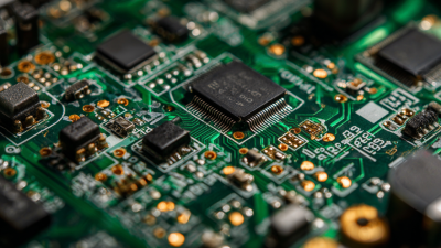
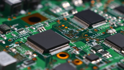
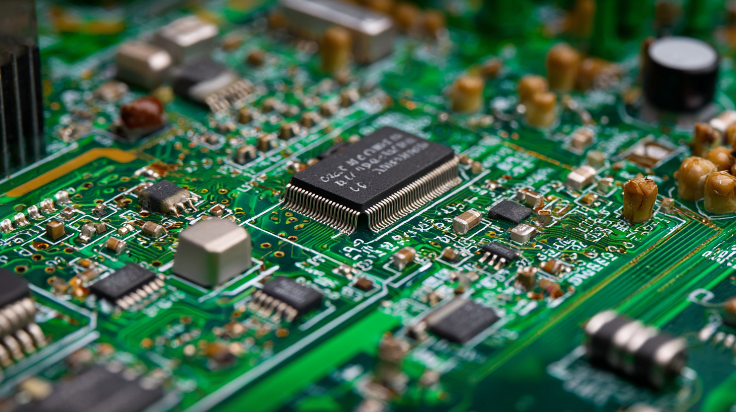
 Printed circuit boards (PCBs) are essential components in electronic devices, serving as the backbone for electrical connections. For beginners, understanding PCBs involves grasping a few key concepts. First, the material used to create PCBs, usually a non-conductive substrate like fiberglass or epoxy resin, is crucial. This substrate is layered with conductive materials, such as copper, which allow for the pathways that connect various electronic components.
Another fundamental aspect is the design process itself, which includes schematic capture and layout design. Schematic capture involves creating a diagram of the circuit, detailing the connections between components. Once the schematic is finalized, the layout design phase begins, where the physical arrangement of components on the PCB is determined. This part is critical since proper spacing and routing can significantly affect the board's performance and reliability, ensuring efficient electrical flow while minimizing interference. By grasping these basic principles, beginners can lay the groundwork for more advanced PCB design techniques.
Essential Tools and Software for PCB Design: A Beginner's Toolkit
When venturing into the world of Printed Circuit Board (PCB) design, having the right tools and software is crucial for beginners. A recent report by ResearchAndMarkets indicates that the global PCB design software market is expected to reach $8.5 billion by 2027, underscoring the growing importance of efficient design tools. Emerging designers can benefit immensely from software like Altium Designer, which is known for its user-friendly interface and extensive features. It allows users to create intricate designs while simplifying complex workflows—a necessity for those starting out.
In addition to Altium, other essential tools include KiCad and Eagle, both of which offer extensive libraries and community support. According to a survey by TechValidate, over 60% of PCB designers reported using these software tools due to their affordability and accessibility. Furthermore, simulation and testing tools, such as SPICE and LTspice, help novices validate their designs in a virtual environment, ensuring functionality before production. These foundational tools not only streamline the PCB design process but also empower beginners to innovate and experiment without the steep learning curve traditionally associated with this field.
Step-by-Step Guide to Creating Your First PCB Layout
Creating your first PCB layout can seem daunting, but by following a structured, step-by-step approach, even beginners can master the basics. Start by defining your project clearly—understanding the functionality and specifications of the circuit is crucial. According to industry reports, over 60% of PCB failures are attributed to design errors, which highlights the importance of careful planning during the layout phase.
Next, utilize PCB design software that suits your needs. Popular tools provide numerous templates and libraries to help streamline the design process. After laying out the schematic, you can begin arranging components on the PCB. A well-organized layout not only optimizes space but also enhances performance. Aim for a design that minimizes signal interference and accommodates future modifications. Research indicates that efficient designs can reduce overall production costs by up to 30%, making the effort invested in learning this skill a worthwhile pursuit for beginners interested in electronics and design.
PCB Design Complexity Over Time
Best Practices in Component Sizing and Placement for Optimal Performance
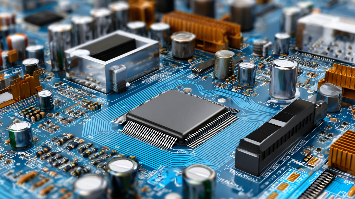
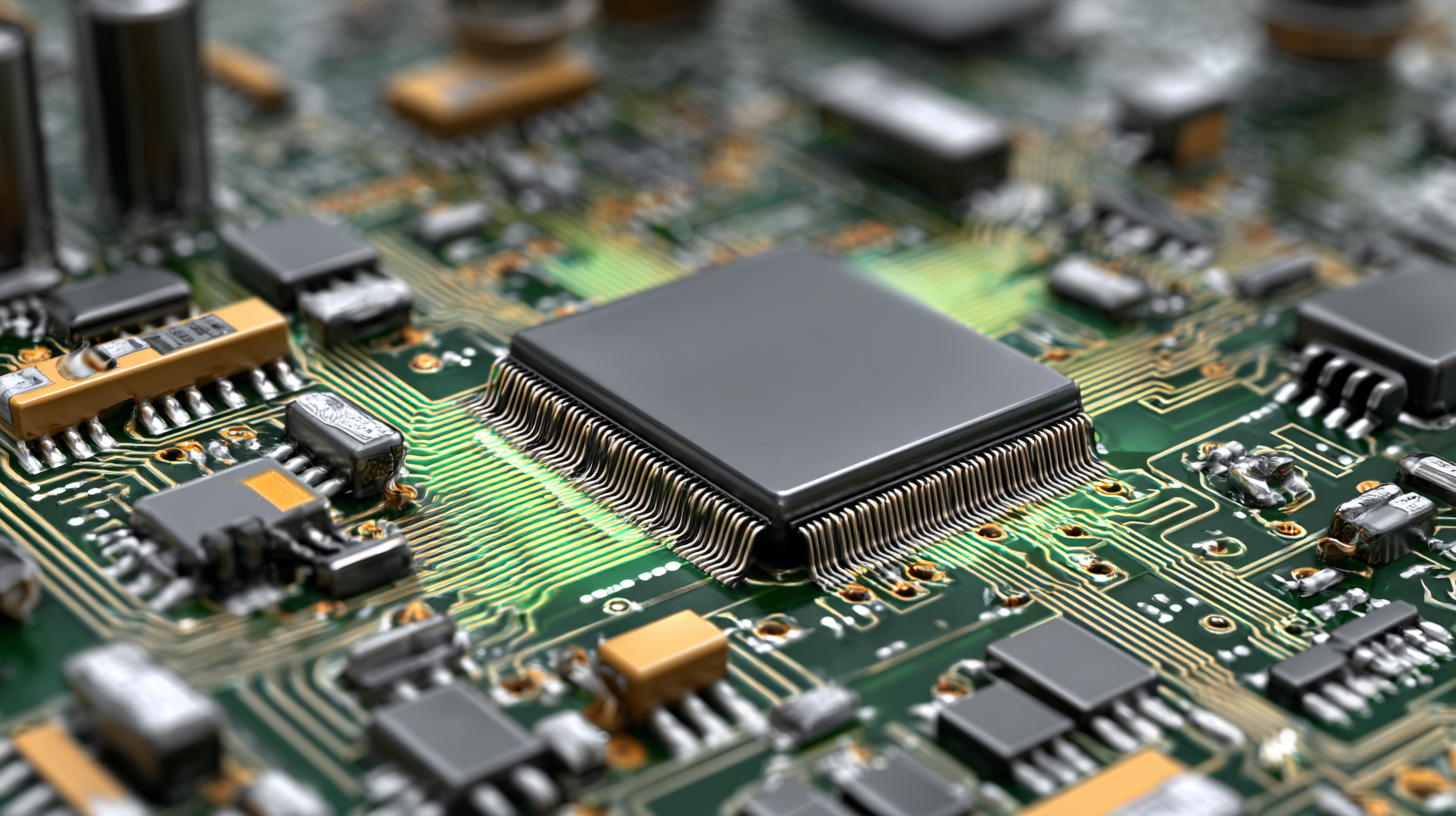
When it comes to printed circuit board (PCB) design, component sizing and placement play crucial roles in achieving optimal performance. According to a recent report by IPC, improperly sized components can lead to issues such as increased power loss and signal integrity problems, which in turn affect the overall functionality of electronic devices. For instance, research indicates that a reduction of even 10% in component size can potentially double the thermal efficiency, making it imperative for designers to meticulously plan the dimensions of each component.
Moreover, the strategic placement of components on a PCB can significantly enhance performance. A study published in the IEEE Transactions on Components, Packaging and Manufacturing Technology emphasizes that proper spacing between components can help mitigate electromagnetic interference, which is pivotal in high-frequency applications. Furthermore, adhering to best practices in component placement can improve manufacturability and simplify the assembly process, contributing to reduced production costs. As highlighted in various industry benchmarks, following optimal design guidelines can lead to a 20% reduction in manufacturing time, ultimately influencing time-to-market and competitive advantage for manufacturers.
Understanding the Basics of Printed Circuit Board Design for Beginners - Best Practices in Component Sizing and Placement for Optimal Performance
| Component Type |
Recommended Size (mm) |
Recommended Placement Distance (mm) |
Optimal Orientation |
Performance Impact |
| Resistor |
0402 |
1.0 |
Horizontal |
Low heat generation |
| Capacitor |
0603 |
2.0 |
Vertical |
Improved stability |
| Inductor |
0805 |
1.5 |
Horizontal |
Critical for filtering |
| Microcontroller |
28-pin |
3.0 |
Vertical |
High processing speed |
| Connector |
2.54 |
2.0 |
Horizontal |
Ease of connection |
Troubleshooting Common PCB Design Errors: Tips for New Designers
 When delving into PCB design, beginners often encounter a range of common errors that can derail projects. Understanding these pitfalls is crucial for developing reliable circuit boards. One prevalent issue is incorrect component placement. Ensure that components are positioned according to the design specifications and double-check their orientations. Proper placement not only aids in functionality but also minimizes unnecessary rerouting.
Another significant area to focus on is signal integrity. Issues such as inadequate trace width or spacing can lead to performance problems. Utilize simulation software to help visualize and analyze potential weaknesses in your design. Make sure to consider the return paths and minimize loop areas to maintain signal quality.
Finally, take advantage of modern advancements in technology. With the rise of AI in PCB design, new tools can streamline your process by identifying potential errors before they escalate. Implementing AI-driven software can significantly enhance your efficiency, allowing you to focus on innovation rather than troubleshooting. As you navigate your design journey, remember that learning from mistakes is part of the process, and utilizing these resources will help you grow as a designer.