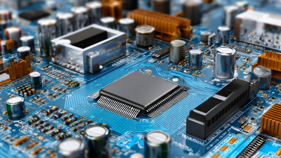
2026 Best PCB Fabrication and Assembly Practices for Innovative Designs?
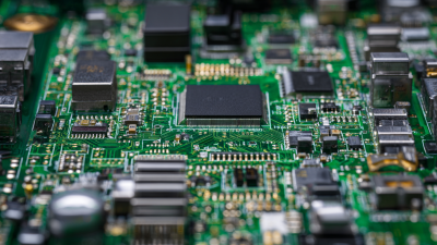
In the rapidly evolving world of electronics, effective PCB fabrication and assembly practices are crucial. As we approach 2026, innovative designs demand new standards and methods. Designers must consider the entire lifecycle of PCB production, from concept to final assembly. Attention to detail is key to achieving high-quality results.
PCB fabrication and assembly require precise techniques. Many projects face unexpected challenges, such as material quality and timing issues. Miscommunication can lead to delays and increased costs. It is essential to address these shortcomings through better planning and execution. Striking a balance between creativity and practicality is vital for success in this competitive field.
Engineers must stay updated on the latest technologies and trends. New manufacturing processes can improve efficiency and reduce waste. However, embracing change can be daunting. Some may hesitate to adopt new methods, fearing disruptions. Yet, adapting to innovative practices can ultimately drive progress in PCB fabrication and assembly, leading to superior designs.
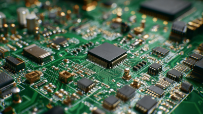
Best Practices for PCB Fabrication in 2026: An Overview
In 2026, the landscape of PCB fabrication is evolving rapidly. Manufacturers must embrace innovative techniques to remain competitive. First, understanding the complexities of material selection is crucial. Different materials affect durability and performance. Choosing the right substrate is key to achieving reliability in diverse applications.
Precision is vital during the fabrication process. Controlled environments can minimize contamination and improve overall quality. However, maintaining such conditions can be challenging. It demands strict adherence to cleanliness protocols. Even minor lapses can lead to defects, impacting device functionality. Thus, continuous evaluation of processes is necessary to enhance efficiency.
Assembly techniques are equally important. Automating assembly can streamline production, but it’s not without risks. It may lead to misalignment or soldering issues, which require careful oversight. Regular training for operators can help in reducing these errors. Ultimately, striking a balance between automation and human skill is necessary for optimal results. A proactive approach to problem-solving will drive future innovations in PCB technology.
Key Considerations in PCB Design for Enhanced Fabrication Efficiency
When designing PCBs, several factors significantly enhance fabrication efficiency. Attention to trace widths is crucial. Wider traces can carry more current, reducing potential overheating. However, overly wide traces may limit space for other features. Striking a balance is necessary.
Component placement is another vital consideration. Grouping similar components together saves time during assembly. Positioning high-frequency components away from noisy parts can help boost performance. Yet, designers must ensure easy access for soldering. If components are too close, assembly could become problematic, leading to errors.
Designers should also focus on PCB layer count. While multilayer boards allow for more complex designs, they can complicate fabrication. Each layer adds cost and time. Basic designs can often be achieved with fewer layers, simplifying the process. However, limiting layers may restrict design potential. Thus, it requires careful deliberation.
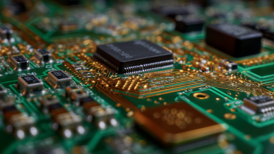
Trends in PCB Assembly Techniques for Innovative Products in 2026
In 2026, PCB assembly techniques are evolving rapidly. Designers are embracing flexible printed circuit boards. These boards can be bent, twisted, or folded, making them ideal for compact devices. Miniature components are also gaining traction. As products get smaller, precision becomes crucial. The challenge lies in maintaining quality while pushing these limits.
New assembly methods are emerging to address these needs. Automated soldering techniques improve speed and accuracy. Yet, there are concerns about ensuring consistent quality. A single error could lead to failures in complex designs. It's essential to reconsider these processes. Inspecting and testing each stage of assembly becomes vital for reliability.
Innovative designs are not just about new technology. They require a reevaluation of traditional methods. While advancements are exciting, they bring challenges that must be faced. Collaboration between engineers and manufacturers can lead to better solutions. Effective communication is key to overcoming potential hurdles. Finding the balance between innovation and practicality is crucial for success.
2026 Best PCB Fabrication and Assembly Practices for Innovative Designs
| Data Dimension |
Description |
Trends in 2026 |
| Material Types |
Flexible, Rigid-Flex, and High-Frequency materials |
Increased use of advanced materials for better performance |
| Manufacturing Technologies |
Laser cutting, 3D printing, and automated assembly |
Higher automation and rapid prototyping processes |
| Assembly Techniques |
Surface mount technology (SMT) and through-hole technology (THT) |
Greater integration of SMT for miniaturization |
| Quality Control |
Automated Optical Inspection (AOI) and X-ray inspection |
Enhanced quality assurance through AI-driven methods |
| Environmental Standards |
Restrictions on hazardous substances (RoHS compliance) |
Stricter regulations pushing for eco-friendly solutions |
| Market Trends |
Growing demand for IoT and smart device applications |
Increased investment in PCBs for innovative technology integration |
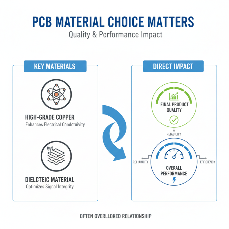
Impact of Material Selection on PCB Quality and Performance Metrics
The choice of materials in PCB fabrication is crucial. It directly affects the overall quality and performance of the final product. For instance, using high-grade copper can enhance electrical conductivity. Meanwhile, selecting the right dielectric material impacts signal integrity. This relationship is often overlooked.
Different projects demand distinct material types. Standard FR-4 might suffice for basic designs. But, for high-frequency applications, options like PTFE are better. However, these advanced materials can be more costly. This raises the question: are the performance benefits worth the extra expense?
Consider the environmental factors too. Temperature fluctuations can stress certain materials. This can lead to unexpected failures. Designing for reliability means reflecting on the choices made during material selection. Balancing cost, performance, and sustainability is challenging but necessary for innovation.
Statistical Analysis of PCB Failures and Reliability in Modern Applications
In the world of PCB design, understanding reliability is crucial. Statistical analysis reveals common failure modes in modern applications. For instance, solder joint fatigue frequently leads to circuit board malfunctions. These failures often result in costly downtime and customer dissatisfaction.
Environmental factors contribute to PCB reliability issues. Temperature fluctuations can cause material expansion and contraction. This can stress solder joints and other connections. Designers should consider these factors early in the design process. Many overlook their significance. They might focus only on aesthetics or performance.
Data shows that a proactive approach can enhance reliability. Investing time in reliability testing pays off. Techniques like thermal cycling tests and moisture resistance assessments can uncover potential weaknesses. Such practices help teams build robust designs. Missing these steps can lead to unexpected challenges later on.
2026 Best PCB Fabrication and Assembly Practices
This chart illustrates the statistical analysis of PCB failures due to various factors for 2026. The data shows that manufacturing defects and design issues are the leading causes of failure, highlighting the need for improved fabrication and assembly practices in innovative PCB designs.