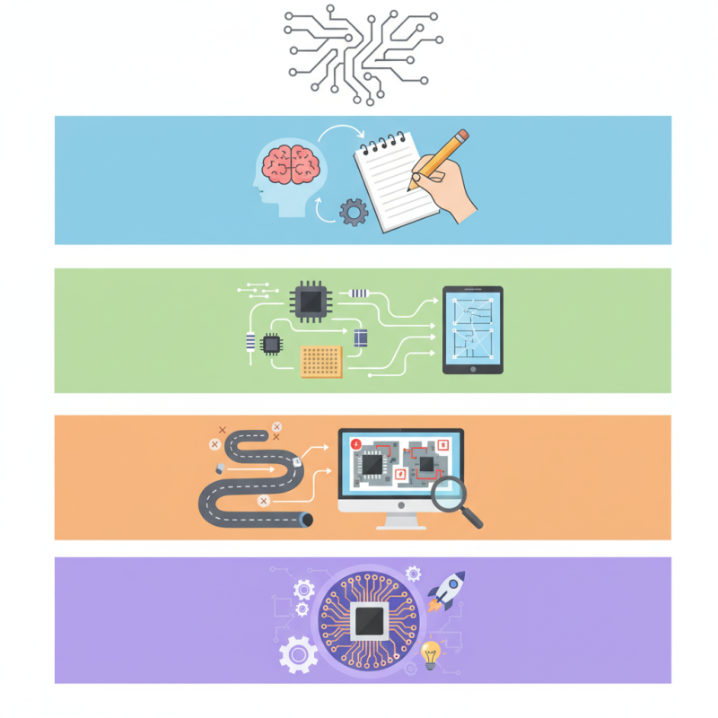
How to Design a PCB Board for Your Electronic Projects?
Designing a PCB board for your electronic projects can be both exciting and challenging. A well-designed PCB board is crucial for the functionality of your project. It serves as the backbone, connecting various components seamlessly.
When creating a PCB board, clarity is key. You must visualize how your components will interact. Sketch layouts on paper before moving to software tools. Mistakes happen. Perhaps you realize a component doesn’t fit as planned. This trial and error is a natural part of the learning curve.
Getting familiar with PCB software can feel overwhelming. Each program has unique features. Take your time to explore these tools. Acknowledge the bumps along the way. Each design iteration teaches valuable lessons. In the end, a functional PCB board emerges, reflecting both your effort and creativity.
Understanding PCB Layout Design Principles for Electronics
Designing a PCB board requires understanding the principles of layout design. The placement of components affects signal integrity and thermal management. Proper spacing between traces can reduce interference. The IPC standard emphasizes that a gap of at least 0.2 mm is essential for reliable designs. Factors like layer count and routing complexity can impact the overall performance.
When arranging components, consider the flow of current. Place power and ground near the edges. This minimizes voltage drops and ensures stability. Use wider traces for power lines to handle higher currents. A common mistake is neglecting to check thermal dissipation. Overheating can lead to device failure. Monitor component temperatures during testing.
**Tip:** Always review your design multiple times. Fresh eyes can catch mistakes overlooked earlier.
Review your schematic before converting it to layout. Errors can propagate into PCB designs. Utilize simulation tools to identify potential signal issues. Don’t ignore the importance of vias and their placement. They can create bottlenecks if not correctly positioned.
**Tip:** Keep your design simple. Complexity increases the chance of mistakes. Aim for clarity in your layout.
Selecting the Right Materials and Components for Your PCB
When designing a PCB, selecting the right materials and components is crucial. The substrate material is the base of your PCB. Common options include FR4, which is cost-effective, and Rogers, which offers better performance. Each material has different characteristics. Consider factors like thermal performance and dielectric constant.
Choosing components requires attention to detail. Look at the specifications of each component. Pay close attention to the voltage and current ratings. Small errors can lead to significant issues later. You might overlook the footprints on the PCB. They must match precisely to ensure proper soldering. Additionally, component placement can affect signal integrity. Take some time to rethink your layout carefully.
Be mindful of your design choices. Sometimes, a cheaper component might save money initially, but it could lead to failures. Testing prototypes is essential. Anticipate potential issues and iterate. Reflect on what can be improved. Room for growth often comes from exploring these imperfections in your design process.
How to Design a PCB Board for Your Electronic Projects? - Selecting the Right Materials and Components for Your PCB
| Component |
Material |
Function |
Recommended Specifications |
| Resistor |
Carbon Film |
Current Limiting |
1/4 Watt, ±5% Tolerance |
| Capacitor |
Ceramic |
Energy Storage |
10µF, 16V |
| LED |
Epoxy |
Indicator Light |
5mm, 20mA |
| Microcontroller |
Silicon |
Control Logic |
32-bit, 48MHz |
| Inductor |
Ferrite Core |
Energy Storage |
10µH, 1A |
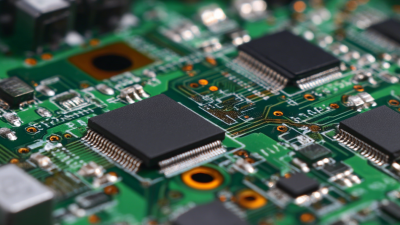
Key Manufacturing Processes in PCB Fabrication and Assembly
Designing a PCB involves understanding several key manufacturing processes. The most important steps include material selection, layer stacking, and etching. Materials like FR-4 are common and offer good insulation. Layer stacking defines the board's complexity. Multilayer boards often have more functionality but increase the manufacturing challenge.
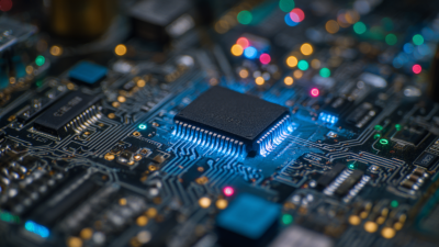
Etching is crucial in forming the circuit paths. It involves removing unwanted copper from the board surface. Precision is key here. If the etching isn't accurate, circuit shorts may occur. This can lead to unexpected failures in your project.
Assembly is another critical process. Components need to be placed accurately on the board. Misalignment can cause serious issues. Soldering follows, and it must be done carefully. Poor solder joints can lead to intermittent connections. This reflects the importance of quality control throughout manufacturing. Mistakes can be costly, so always review your design thoroughly.
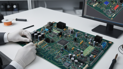
Best Practices for Testing and Troubleshooting Your PCB Design
Testing and troubleshooting your PCB design is crucial for success. According to industry reports, up to 30% of PCBs fail during testing due to design flaws. These flaws often stem from inadequate planning and assumptions made during the design phase. Every trace and component layout should be meticulously reviewed. This includes checking traces for shorts or opens and ensuring there is no unintentional interference between circuits.
Using tools like oscilloscopes and logic analyzers helps visualize the voltage levels and signal integrity. It allows for early detection of issues such as ground bounce or crosstalk. Regularly reviewing test results is just as vital. Data shows that 15% of designs might need rework after testing. This means lessons learned from one project should refine processes in subsequent designs. Remember, a single error can lead to significant delays and increased costs.
Make sure to document all testing procedures and results. This keeps a record of what worked and what didn't. Sometimes, teams forget simple issues like missing components or incorrect orientations. These small mistakes can lead to larger, unforeseen problems later. Regularly reflecting on your troubleshooting process can reveal recurring pitfalls. Each project teaches something new, and that knowledge creates a stronger foundation for future designs.