How to Design PCB for Maximum Efficiency and Cost Savings?
In the highly competitive world of electronics, the ability to design PCB efficiently is critical. Dr. Emily Chen, a leading expert in PCB design, once stated, "Effective PCB design can significantly reduce costs while boosting performance." This highlights the importance of smart strategies in creating PCBs that not only meet technical requirements but also align with budget constraints.
Maximizing efficiency in PCB design involves understanding materials, layout, and manufacturing processes. Poorly planned designs can lead to increased production costs and delays. As engineers, we must focus on optimizing the placement of components to reduce trace lengths. This can enhance performance and lower manufacturing costs.
Furthermore, taking a holistic approach to design PCB involves considering future scalability. While immediate cost savings are appealing, overlooking long-term implications may lead to inefficiencies. Continuous improvement in design processes can lead to sustainable savings. Investing time in research and development helps us avoid common pitfalls and ensures that designs stand the test of time. Each decision made in the design phase can dramatically impact both efficiency and expense.
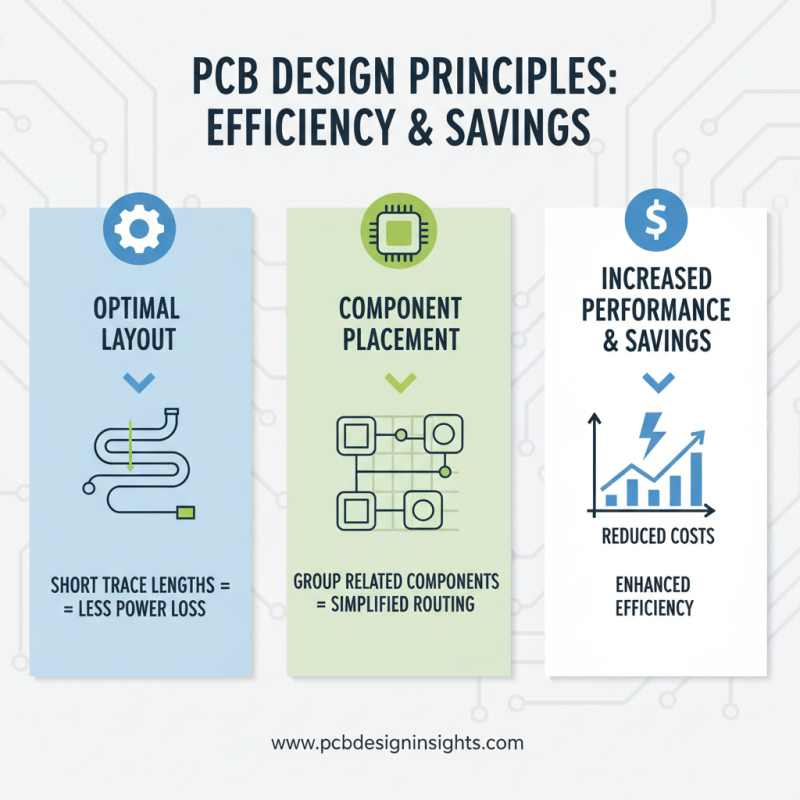
Understanding PCB Design Principles for Efficiency and Savings
When designing PCBs for efficiency and cost savings, one must grasp key design principles. Optimal layout is crucial. Each trace should minimize length to reduce resistance. This can lead to less power dissipation. Prioritize component placement carefully. Group related components together. This can simplify routing and enhance performance.
Thermal management is another vital aspect. Components that generate heat need ample space and proper heat sinks. Overheating can lead to failures, which drive up costs. Furthermore, consider the use of multilayer boards. They allow for more complex designs without taking up excessive space. However, multilayer boards can be costly. Thus, weigh their benefits against the budget.
Designing for manufacturability is essential. Providing clear guidelines can prevent errors. Complex designs often lead to miscommunication with manufacturers. Hence, maintain simplicity where possible. Common pitfalls include overestimating the capabilities of PCB manufacturers. Always check their specifications. Balancing efficiency and cost requires careful consideration and sometimes, reevaluation of the design choices made.
Selecting the Right Materials for Cost-Effective PCB Production
Selecting the right materials for cost-effective PCB production is crucial. The choice of materials directly impacts performance and expenses. High-quality materials can enhance signal integrity, but they can also inflate costs. It’s essential to strike a balance between durability and budget.
Copper thickness is a key factor. Thicker copper layers can handle higher currents, leading to increased reliability. However, they are more expensive. Consider your project requirements carefully. Will thicker copper truly benefit your design? For low-power applications, thinner layers may suffice, saving costs.
Consider using FR-4 as a base material. It’s widely used and cost-effective. However, it might not perform well in high-frequency applications. Research alternatives like Rogers materials or aluminum for specific needs. Each option has its pros and cons. Evaluate them thoroughly.
Tips: Always prototype with different materials. This allows you to test performance without committing to a large production run. Use simulation tools to predict how materials will behave in real-world conditions. Collect data and make informed decisions based on your findings.
PCB Material Efficiency and Cost Analysis
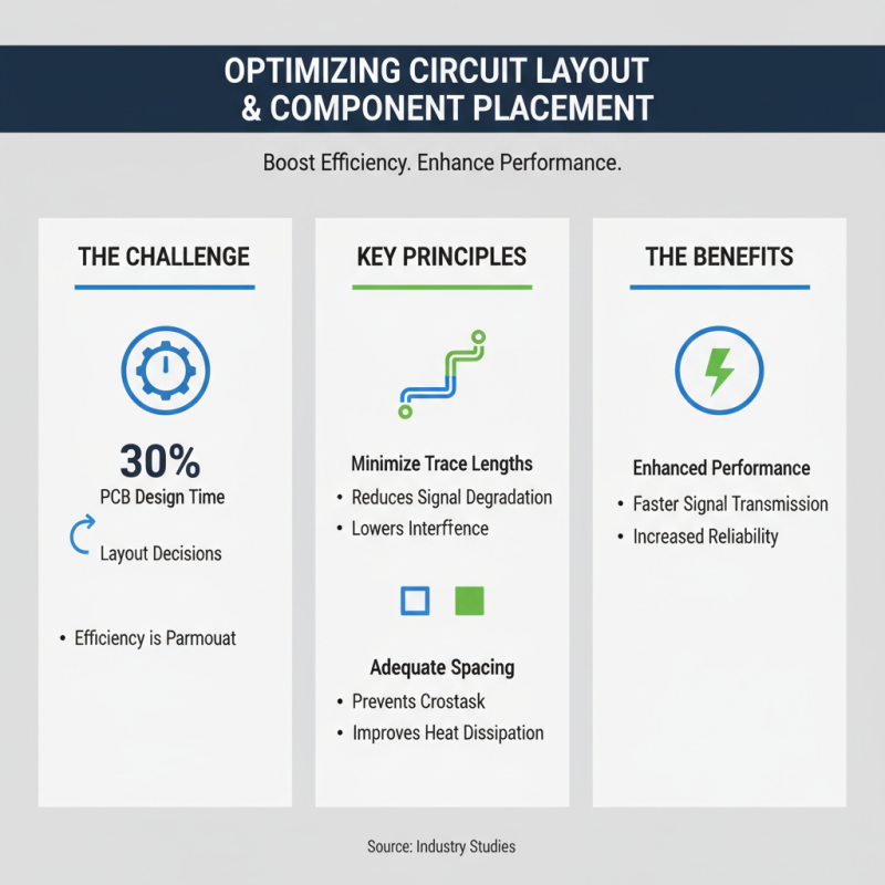
Optimizing Circuit Layout and Component Placement for Performance
When optimizing circuit layout and component placement, efficiency is paramount. Studies indicate that approximately 30% of PCB design time can be attributed to layout decisions alone. Key considerations include minimizing trace lengths and ensuring adequate spacing between components. Shorter traces reduce signal degradation and interference, ultimately enhancing performance.
Another critical aspect is the placement of components. Centralizing high-frequency components can prevent noise and crosstalk issues. A report from industry experts suggests that effective component placement can improve signal integrity by up to 15%. Additionally, clusters of related components can simplify the routing process, leading to shorter paths and less complexity.
However, it's essential to reflect on potential pitfalls. Sometimes, designers focus too heavily on aesthetics rather than functionality. This can lead to challenging thermal management and efficiency issues. Balancing layout design with practical performance metrics requires careful consideration and reflection. Incorporating iterative testing throughout the design process can help identify these challenges early.
Implementing Design Rules to Minimize Manufacturing Costs
Designing a PCB (Printed Circuit Board) with a focus on minimizing manufacturing costs can significantly enhance efficiency. Implementing design rules is crucial in achieving this goal. According to a report by IPC, effective design practices can reduce costs by up to 30%. By adopting these practices, designers can avoid expensive revisions and delays during production.
One effective tip is to standardize component footprints. This approach can reduce setup times and enhance manufacturing yield. Additionally, using a limited number of components can streamline the procurement process, thus lowering overall costs. Ensure all components are readily available, as this can save time and funds during production.
Another aspect to consider is the layout. The placement of components directly impacts the manufacturing processes. A well-organized PCB layout can minimize the number of vias and trace lengths, further cutting costs. Poor layouts often lead to increased complexity, which can drive prices higher. Always aim for simplicity without compromising functionality. Also, revisiting and refining design iterations can uncover potential savings and improve overall designs.
Testing and Iterating PCB Designs for Maximum Efficiency
When designing PCBs, testing and iterating is crucial for achieving maximum efficiency. Each iteration reveals insights into performance and functionality. Prototyping can uncover flaws in design. It's vital to address these flaws before finalizing a product.
Testing should be thorough and varied. Use thermal analysis to check heat distribution. This can prevent potential failures. Consider electrical testing for signal integrity. Check for noise issues, as they can affect overall performance.
Tips: Engage in peer reviews of your design. Fresh eyes can catch overlooked mistakes. Incorporate feedback into your next iteration. Document every test result meticulously. This information is invaluable for future projects. Remember, each design is a learning opportunity. Embrace the process of iteration.