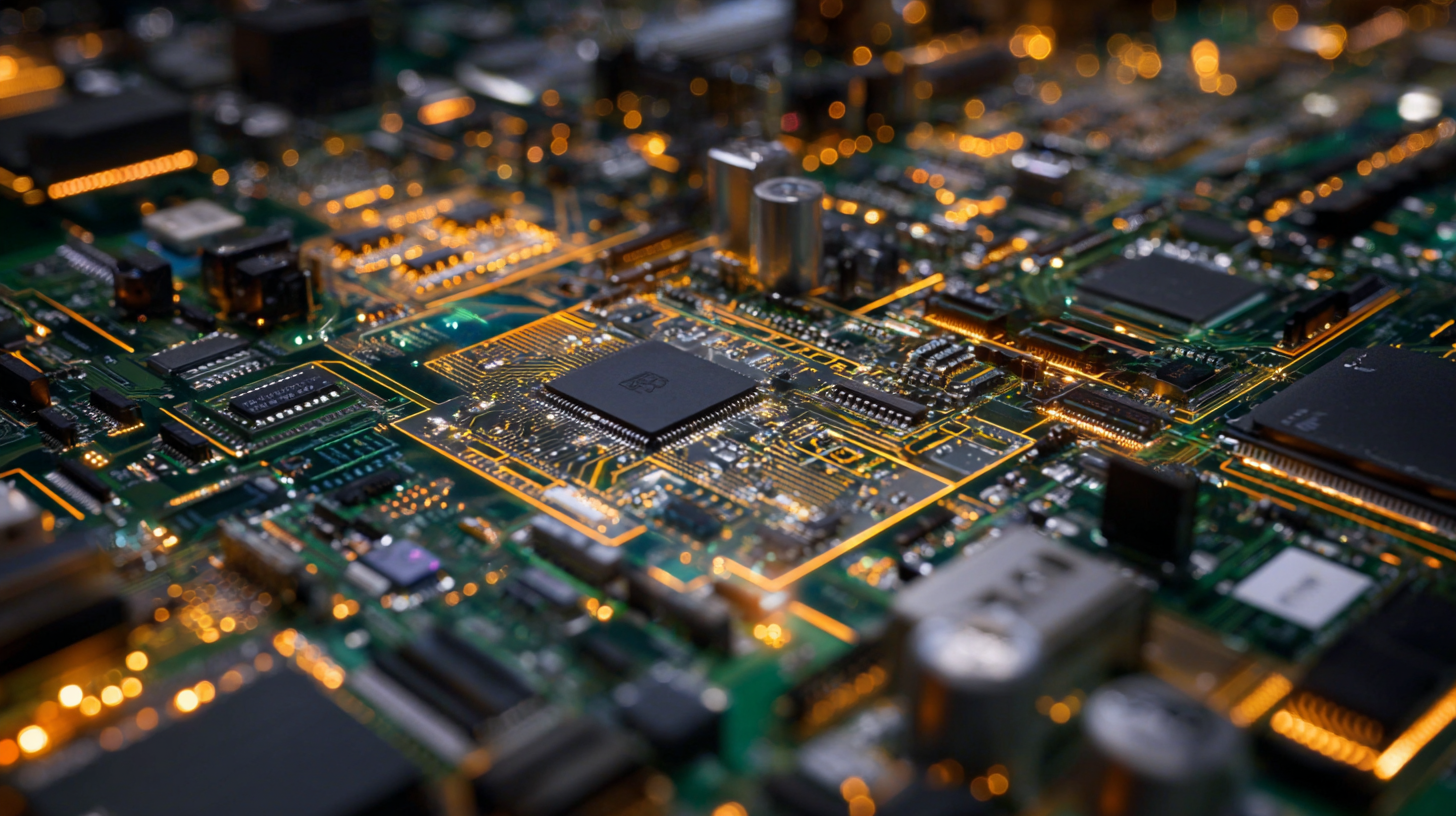
Unlocking Efficiency: Advanced Techniques in Circuit Board Manufacturing for Modern Electronics
In the rapidly evolving landscape of modern electronics, the demand for high-performance and efficient circuit board manufacturing has never been more critical. As devices become increasingly sophisticated, manufacturers are compelled to innovate and adopt advanced techniques that not only enhance the quality and reliability of circuit boards but also streamline production processes.
This article explores the various methods and technologies that are reshaping the circuit board manufacturing industry, enabling companies to meet the heightened expectations of consumers and the marketplace.
From automation and precision engineering to innovative materials and design practices, these advancements are essential for fostering a competitive edge in a sector characterized by swift technological advancements and shifting consumer preferences.
As we delve into the intricacies of circuit board manufacturing, we will highlight how these techniques are unlocking unparalleled efficiency and paving the way for the next generation of electronic devices.
Innovative Materials: Enhancing Circuit Board Performance and Durability
The demand for durable and high-performance circuit boards has never been greater in the modern electronics landscape. Innovative materials have emerged as a focal point in enhancing the performance and longevity of these essential components. Recent research indicates that the integration of lignocellulose nanofibrils (LCNF) as substrates in printed circuit boards (PCBs) can significantly improve sustainability and performance metrics. LCNF not only offers a biodegradable alternative but also enhances the mechanical properties of PCBs, making them more resilient to environmental stressors.
In parallel, advancements in thermal management techniques are crucial for the reliability of electronic components. Studies from the National Renewable Energy Laboratory demonstrate that new electronics packaging can lead to longer-lasting components that operate efficiently even under high thermal loads. These improvements are vital as the industry trends towards thinner and lighter devices while maintaining high functionality.
Furthermore, the development of magnetic transistors captures attention for its potential to simplify circuit designs, paving the way for faster, more energy-efficient electronic systems. This innovation aligns with the increasing need for efficient energy usage, as advancements continue to integrate smart materials and technologies, underscoring the evolving landscape of circuit board manufacturing amidst heightened performance demands.
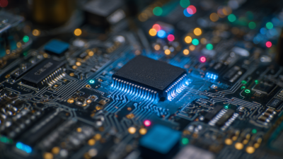
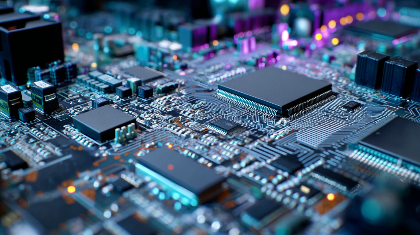
Unlocking Efficiency in Circuit Board Manufacturing
Streamlined Design Processes: Automation in PCB Layout and Prototyping
The design and prototyping of printed circuit boards (PCBs) have evolved significantly with the integration of advanced automation techniques. Streamlined design processes, facilitated by sophisticated software tools, enable engineers to create intricate layouts with remarkable precision and efficiency. By automating routine tasks such as component placement and routing, designers can focus on optimization and innovation, ultimately enhancing product functionality and reducing time to market.
Furthermore, automated prototyping technologies, including 3D printing and rapid PCB fabrication systems, have revolutionized the testing phase of circuit board manufacturing. These techniques allow for swift iteration and modification of designs, enabling engineers to conduct thorough testing and validation without the lengthy delays associated with traditional prototyping methods. Consequently, the modern electronics landscape benefits from quicker turnaround times and the ability to respond to market demands more effectively, all made possible through the intelligent application of automation in PCB design and prototyping processes.
Advanced Manufacturing Techniques: 3D Printing and Laser Cutting in PCB Production
The rise of 3D printing and laser cutting technologies is transforming the landscape of PCB manufacturing for modern electronics. Start-ups like LPRINT are at the forefront of this revolution, aiming to redefine how circuit boards are designed and produced. With innovations in 3D electronic printing, manufacturers can create complex geometries that were previously difficult to achieve, meeting the growing demands for lightweight and structurally optimized designs. This advancement not only enhances design flexibility but also accelerates prototyping, reducing time-to-market for new electronic products.
Laser cutting, on the other hand, complements these 3D printing advancements by enabling precise fabrication of flexible printed electronics. By employing laser-enabled processes, manufacturers can produce large-area circuits with integrated functional devices efficiently and accurately. Together, these advanced techniques address the challenges of miniaturization and customization in electronics, paving the way for innovative applications such as wearable technology and other body-conformable devices. As the industry moves towards smarter manufacturing solutions, the synergy of 3D printing and laser cutting will play a crucial role in unlocking new efficiencies in PCB production.
Quality Control Measures: Implementing Real-Time Monitoring for Fault Detection
In today's fast-paced electronics landscape, ensuring product quality is paramount, which is why implementing real-time monitoring for fault detection has become a cornerstone strategy in circuit board manufacturing. According to a recent industry report by IPC, nearly 70% of manufacturing defects can be traced back to process variations, underscoring the critical need for robust quality control measures. By employing advanced techniques such as automated optical inspection (AOI) and X-ray analysis, manufacturers can proactively identify defects in real-time, significantly reducing waste and rework costs.
Moreover, the integration of Internet of Things (IoT) technologies into manufacturing processes enables continuous data collection and analysis, facilitating immediate feedback on production quality. A study published by Deloitte suggests that companies leveraging real-time monitoring systems can reduce their defect rate by as much as 30%, leading to substantial cost savings and improved customer satisfaction. As the demand for high-quality electronics continues to rise, investing in sophisticated quality control measures will be essential for manufacturers looking to stay competitive in this evolving market.
Sustainable Practices: Eco-friendly Approaches in Circuit Board Manufacturing
In the rapidly evolving field of circuit board manufacturing, sustainable practices have become a critical focus for both manufacturers and consumers. According to a report by the International Electronics Manufacturing Initiative (iNEMI), approximately 70% of electronic waste arises from circuit boards, highlighting an urgent need for eco-friendly manufacturing processes. Industries are now adopting technologies such as lead-free soldering and the use of recyclable materials to mitigate their environmental impact. Companies that implement these practices not only reduce waste but also comply with strict regulations like the RoHS directive, which limits harmful substances in electronic components.
Moreover, integrating green practices can lead to increased efficiency and cost savings. A study by the Environmental Protection Agency (EPA) showed that manufacturers implementing sustainable approaches could reduce their operational costs by up to 15%. For example, the adoption of closed-loop recycling systems allows manufacturers to reclaim materials from old circuit boards and reintroduce them into the production cycle. This not only conserves natural resources but also promotes a circular economy within the electronics industry. As sustainability becomes a key consumer demand, businesses that proactively embrace these eco-friendly methods are likely to enhance their competitiveness in the modern market.
Unlocking Efficiency: Advanced Techniques in Circuit Board Manufacturing for Modern Electronics
Sustainable Practices: Eco-friendly Approaches in Circuit Board Manufacturing
| Technique |
Description |
Eco-friendly Aspect |
Efficiency Improvement (%) |
| High-Density Interconnect (HDI) |
Increases routing density without enlarging the board size. |
Reduces material usage and waste. |
25% |
| Flexible Circuit Boards |
Allows for compact designs and integration into small spaces. |
Using bio-based materials reduces environmental impact. |
30% |
| Zero-Defect Manufacturing |
Aims to eliminate defects to enhance the production quality. |
Less waste through better quality control systems. |
40% |
| Lead-Free Soldering |
Utilizes solder materials that do not contain lead. |
Safer for both workers and the environment. |
10% |
| Recyclable Materials |
Use of materials that are easily recyclable after product lifespan. |
Minimizes landfill waste. |
15% |