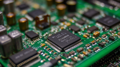
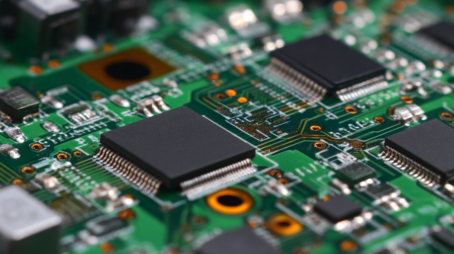
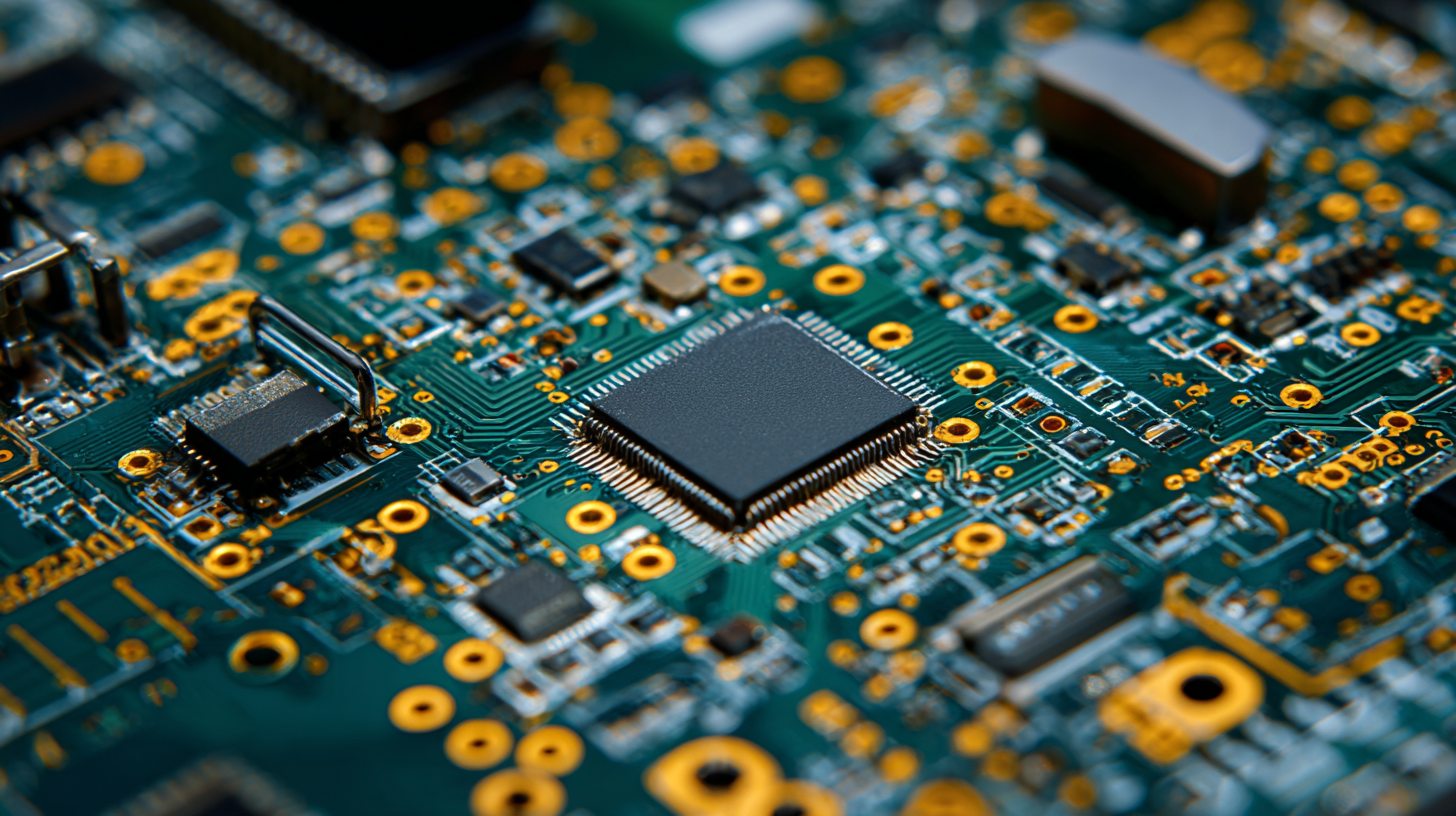
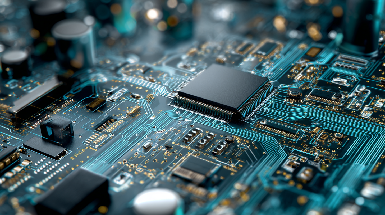
How to Efficiently Design and Manufacture PCB Circuit Boards for Your Projects
The efficient design and manufacturing of PCB circuit boards have become vital for the success of electronic projects, as the global PCB market is projected to reach approximately $80 billion by 2025. With the rapid advancement of technology and an increasing demand for miniaturization and enhanced functionality in electronic devices, optimizing the PCB design process is crucial. According to recent industry reports, incorporating best practices in PCB design can reduce production costs by up to 30% while improving time-to-market by up to 50%. Understanding the intricate relationships between design, materials, and manufacturing processes can empower engineers and designers to create more reliable and efficient PCB circuit boards, ultimately leading to more successful product launches and greater market competitiveness. This article aims to guide you through the essential steps for achieving excellence in PCB design and manufacturing, harnessing the latest trends and technologies for your projects.
Essential Steps for Designing PCB Layouts with Optimal Performance
Designing a PCB layout with optimal performance involves several essential steps. First, understanding the requirements of your project is crucial. This includes determining the electrical parameters and constraints needed for your circuit. Create a detailed schematic diagram that accurately reflects the system you are working on. This will serve as the foundation for your PCB layout, guiding you in component placement and interconnections.
Next, focus on component placement, ensuring minimal signal interference and efficient routing paths. Keep in mind the principles of signal integrity and thermal management; place sensitive components away from high-frequency or high-power elements. After finalizing the placement, you can proceed to route the connections, prioritizing short and direct paths while avoiding unnecessary vias. Properly managing ground and power planes also enhances performance by minimizing noise and maximizing reliability in your design. Through careful planning and execution, you can achieve a PCB layout that not only meets but exceeds performance expectations for your projects.
PCB Design Efficiency: Time Spent on Each Step
Key Considerations for Selecting Materials and Components in PCB Manufacturing
When designing and manufacturing PCB circuit boards, selecting the right materials and components is critical for ensuring performance, reliability, and cost-effectiveness. According to a report by IPC (Institute of Printed Circuits), up to 70% of PCB failures can be attributed to poor material selection. Therefore, understanding the properties of different materials can significantly affect the lifespan and durability of the final product. For instance, using high-frequency laminates can enhance signal integrity in RF applications, while FR-4 remains a popular choice for general-purpose due to its balance of cost and performance.
Moreover, the choice of components impacts both manufacturability and functionality. A study conducted by IHS Markit revealed that the global PCB market is projected to reach $78.4 billion by 2024, emphasizing the importance of selecting components that not only meet electrical requirements but also align with industry standards. Factors such as thermal management, component size, and end-use application should be prioritized during the selection process. By considering these parameters, designers can optimize their PCB designs for efficiency and reliability, ultimately leading to successful project outcomes.
Efficient Techniques for PCB Prototyping and Testing Before Mass Production
Prototyping and testing are critical steps in the efficient design and manufacture of PCB circuit boards. By creating prototypes, designers can validate their ideas and pinpoint any flaws before committing to mass production. Utilizing tools like CAD software for PCB design allows for rapid iterations, enabling teams to modify layouts quickly and test various configurations. Moreover, 3D printing of circuit boards can provide a tangible model for testing physical fit and component placement, streamlining the development process.
Once a prototype is ready, thorough testing is essential to ensure functionality and reliability. Techniques such as Automated Optical Inspection (AOI) and X-ray inspection can identify manufacturing defects that may not be visible to the naked eye. Additionally, performing electrical tests under different operating conditions helps confirm that the PCB will perform as expected in real-world applications. By integrating these prototyping and testing methodologies, engineers can drastically reduce the risk of failures during mass production, ensuring a smoother transition from design to manufacture.
Best Practices for Collaborating with PCB Manufacturers and Suppliers
Collaborating effectively with PCB manufacturers and suppliers is crucial for the success of your projects. First,
clear communication is paramount. Before starting the manufacturing process, provide detailed specifications, including
design files, material preferences, and necessary certifications. Establishing a consistent line of communication helps address potential issues early,
ensuring that both parties are on the same page regarding timelines, costs, and quality expectations.
Additionally, building a strong relationship with your chosen manufacturer can lead to more advantageous outcomes. Engaging with suppliers who
are willing to offer insights or suggestions about your design can significantly improve the efficiency of the process. Being open to feedback and
adaptable in your approach fosters a collaborative atmosphere, which often results in better quality circuit boards and can even help reduce production costs. Regularly reviewing
performance metrics and keeping the manufacturer updated on any design changes will further streamline future collaborations.
Cost-Effective Strategies for Scaling Up PCB Production in Your Projects
When scaling up PCB production for projects, cost-effectiveness becomes a crucial consideration. According to a report by IPC, the global PCB market is expected to reach $83 billion by 2027, driven by increasing demand in sectors such as automotive and consumer electronics. One of the most effective strategies for reducing costs is to optimize design for manufacturing (DFM). By utilizing DFM principles, engineers can minimize the number of layers and reduce the complexity of designs, leading to significant savings in material costs and production time.
Additionally, embracing automation in the manufacturing process can lead to a substantial decrease in labor costs and production errors. A study from Technavio highlights that automated PCB assembly can cut production costs by up to 30%, which directly impacts profitability during large-scale manufacturing. Furthermore, establishing long-term relationships with suppliers can yield better pricing and more favorable terms, ultimately enhancing the project's overall efficiency. By implementing these strategies, project managers can not only achieve cost savings but also maintain high-quality standards as they scale their PCB production.