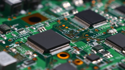
Essential Tips for Designing Printed PCB Efficiently?
In the world of electronics, designing an efficient printed PCB is crucial. Expert John Doe, a renowned figure in printed PCB development, once stated, "The design process can make or break a product." His insight highlights the intricacy and importance of optimal design techniques.
When creating a printed PCB, several factors demand attention. Component placement, layout, and routing all influence functionality. For instance, improper placement can cause signal interference, leading to malfunctions. Attention to detail can save time and resources in the long run. Engineers often face hurdles during design phases, prompting them to rethink their strategies. The learning curve in printed PCB design can be steep, yet essential for innovation.
Additionally, using advanced software tools can aid in achieving better designs. However, relying solely on technology can sometimes lead to overlooking critical details. Hence, a balance between software assistance and manual oversight is needed. Ultimately, an effective printed PCB design is rooted in creativity and careful planning.
Understanding the Basics of PCB Design Principles
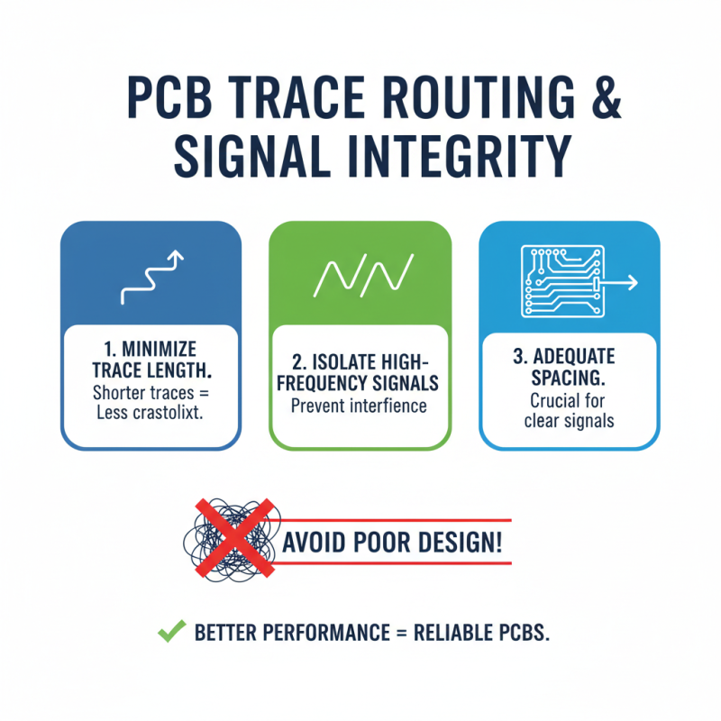
Designing printed circuit boards (PCBs) requires a solid grasp of foundational principles. Start by understanding the layout. Each component should be placed for optimal connectivity. Think about signal integrity. Poor placement can lead to noise and interference. Keep high-frequency components together. Use short traces to minimize electromagnetic interference.
Next, consider the power distribution. A well-design power plane is essential. It should cover the entire area of the PCB for even distribution. Many designers overlook this aspect, leading to overheating issues. Ensure your vias are of appropriate size. Small vias can restrict current flow. Moreover, don't ignore thermal management. It’s easy to forget about heat dissipation when focusing on circuit functionality.
Lastly, maintain a balance between complexity and simplicity. Often, a more complex design may not be necessary. Strive for clarity in your design. Overly complicated layouts can confuse assembly processes. Regularly evaluate your designs. Seek feedback from peers to identify blind spots. Reflection is key to improving your PCB design skills.
Essential Tips for Designing Printed PCB Efficiently
The chart above illustrates the efficiency scores associated with various essential PCB design principles. Each principle is critical to ensuring that the PCB is designed efficiently, minimizing errors while optimizing performance.
Choosing the Right Design Software for PCB Layout
Choosing the right design software for PCB layout is critical for efficient printed circuit board design. A recent survey by IPC reported that over 75% of engineers believe design software significantly impacts project timelines. Therefore, selecting an intuitive tool can enhance productivity levels. Some software options offer a user-friendly interface, but many still present a steep learning curve.
Consider the specific features that fit your project needs. Look for flexible routing capabilities which help in complex layouts. Powerful simulation tools can also save time during testing phases. An effective software package should reduce iterations and errors. However, engineers often report frustration with features that are difficult to navigate. Challenges like these can slow down the design process, defeating the software's purpose.
Market research indicates that application integration is growing in importance. About 60% of professionals find it essential to combine their PCB design tools with other engineering software. This approach streamlines collaboration but can also lead to integration issues. Compatibility is crucial, yet it remains an ongoing struggle. Choosing software with these capabilities can enhance workflow and efficiency, but make sure to weigh the potential hurdles.
Key Considerations for Efficient Component Placement
Efficient component placement is crucial in printed circuit board (PCB) design. Research indicates that improper placement can increase manufacturing costs by up to 30%. The goal is to ensure functionality while minimizing costs and complexities.
One essential factor is maintaining a clear signal path. Grouping components based on their function helps reduce trace lengths. For instance, placing decoupling capacitors close to power pins can enhance reliability. Data from IPC standards suggest that an optimal trace length can minimize power loss and increase system efficiency. However, many designers overlook this detail, leading to potential signal integrity issues.
Thermal management is another critical consideration. Components generating heat should be spaced adequately to allow airflow. Studies show that improper thermal placement can reduce component lifespan by 50%. Additionally, it's vital to balance component sizes and placement alignment. Aesthetics matter, but practicality must prevail. Ignoring these aspects can result in boards that are not only inefficient but also harder to manufacture. The challenge lies in creating boards that are both functional and efficient, while maintaining a design that is practical for assembly. Efficient component placement requires attention to detail and a willingness to adapt designs as new data emerge.
Essential Tips for Designing Printed PCB Efficiently
| Consideration |
Description |
Impact on Efficiency |
| Component Placement |
Strategic positioning of components for optimal connection paths. |
Reduces signal delays and enhances performance. |
| Layer Count |
Choosing the right number of layers to balance complexity and cost. |
Affects manufacturing costs and design complexity. |
| Trace Width |
Determining suitable trace widths for current carrying capability. |
Ensures reliability and minimizes heat generation. |
| Ground Plane Design |
Utilizing ground planes for noise reduction and signal integrity. |
Improves overall circuit performance. |
| Prototyping |
Creating prototypes to test design before final production. |
Identifies issues early, reducing costs and reworks. |
Tips for Testing and Iterating Your PCB Design for Optimization
Testing and iterating your PCB design is crucial for achieving optimal performance. Start by creating a prototype based on your initial design. This helps you identify potential issues early. Use simulation software for stress testing under various conditions. However, these simulations may not capture every real-world variable. You might find discrepancies between expected and actual performance.
Once the prototype is ready, conduct thorough testing. Measure key parameters like signal integrity and power consumption. Analyze how your PCB responds to heat and interference. Gather data meticulously; it can be easy to overlook small details. Small errors in your measurements might lead to significant issues later. After testing, review your findings critically. Don't hesitate to rethink your layout or component choices based on the results.
Iteration is where innovation happens. It is not just about fixing problems but about enhancing design efficiency. Consider feedback from colleagues and end-users. Sometimes their insights can reveal flaws you didn't see. Some design aspects can be subjective, leading to debates. Emphasize open communication throughout the process. Each version should serve as a stepping stone toward a better product. Embrace this cycle of testing and refinement for your PCB designs to thrive.