10 Essential Tips for Effective PCB Board Design
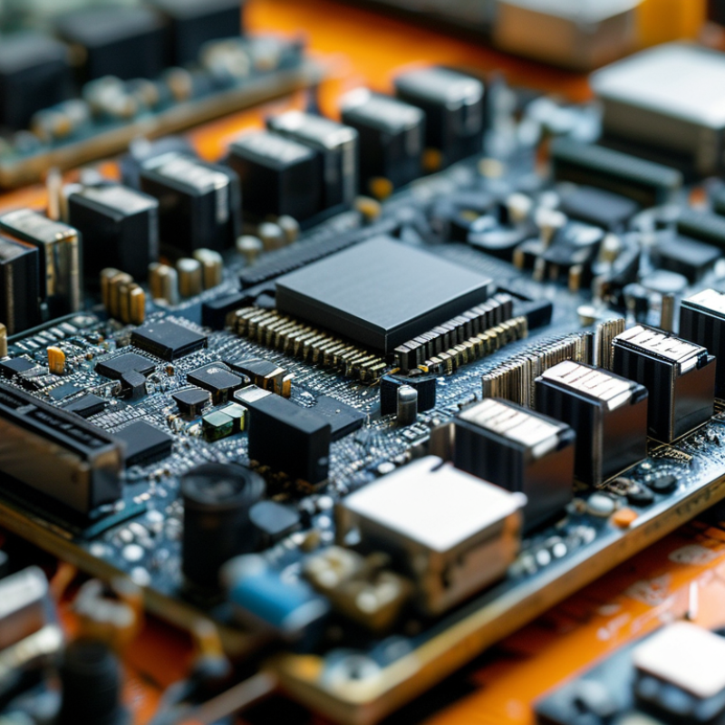
In the world of electronics, effective PCB board design is crucial. A well-designed PCB can enhance performance and reliability. Unfortunately, many designers overlook essential aspects, leading to costly errors. By understanding these pitfalls, we can create better designs.
When embarking on PCB board design, it's vital to consider the layout, components, and signal integrity. Each decision impacts the overall functionality. For instance, proper component placement can reduce interference. Yet, many newcomers ignore these details, ending up with faulty circuits.
The journey of PCB board design is filled with challenges, but it also invites innovation. Adopting best practices can improve our designs significantly. Focusing on real-world limitations and embracing feedback fosters a culture of learning. Ultimately, mastering PCB board design is an ongoing process that demands attention to detail and adaptability.
Understanding PCB Basics and Key Terminology
Understanding the basics of PCB design is crucial for anyone in the electronics field. PCB, or Printed Circuit Board, serves as the backbone of most electronic devices. According to a 2023 industry report, the global PCB market is projected to reach $83 billion by 2027, signifying its importance. Familiarity with key terminology such as vias, traces, and layer stacks is essential. Vias connect different layers, while traces conduct electricity. An understanding of these components enhances your designs.
Tip 1: Ensure proper trace width to reduce resistance. Tools like IPC-2221 provide guidelines to calculate widths based on the current load. This can prevent overheating.
Tip 2: Focus on spacing—improper distances can lead to shorts. The IPC-2222 standard suggests specific distances between components. Adhering to these can mitigate failures in design.
Reflecting on these elements can significantly enhance functionality. Errors in design often occur due to oversight in spacing and trace management. Continuous education in PCB standards helps in addressing common pitfalls and maintaining design integrity.
10 Essential Tips for Effective PCB Board Design - Understanding PCB Basics and Key Terminology
| Tip Number |
Tip Title |
Description |
| 1 |
Understand Your Requirements |
Before designing, clarify the specifications and functionalities of the PCB. |
| 2 |
Component Placement |
Optimize component layout to minimize trace lengths and enhance performance. |
| 3 |
Proper Grounding |
Ensure a solid grounding strategy to reduce noise and enhance signal integrity. |
| 4 |
Thermal Management |
Consider heat dissipation methods during design to prevent overheating. |
| 5 |
Signal Integrity |
Use controlled impedance and appropriate trace widths to maintain signal quality. |
| 6 |
Design Rules Check |
Run DRC to catch spacing, trace width, and other layout errors early. |
| 7 |
Test Point Placement |
Include test points for easy debugging and verification of circuits. |
| 8 |
Use of Via Types |
Select appropriate via types based on current capacity and space constraints. |
| 9 |
Empower Design for Manufacturability |
Consider manufacturing limitations to streamline production and assembly. |
| 10 |
Documentation and Revision Control |
Maintain accurate documentation and version control throughout the design process. |
Choosing the Right Material for Your PCB Design
Choosing the right material for your PCB design is crucial. Different materials provide unique properties, affecting performance and durability. For instance, FR-4 is a common choice due to its excellent insulating properties and cost-effectiveness. However, when high-frequency performance is needed, consider using materials like Rogers or Teflon. These materials offer lower dielectric loss, essential for high-speed applications.
Another factor is thermal management. Copper-filled substrates can enhance heat dissipation, aiding in the prevention of overheating. According to a recent industry report, PCBs with improved thermal properties can extend product lifespan by up to 30%. This is significant, given the rising demand for durable electronics.
When selecting materials, think about your project's specific needs. Are you targeting a low-cost product? Or do you need high performance? Remember that sometimes, a more expensive material can save costs in the long run by reducing failures.
Tip: Always analyze the trade-offs between material cost and performance. Look into detailed specifications. Staying informed helps in making better decisions. Use online resources to compare materials effectively.
Designing Effective Layouts for Signal Integrity
Designing effective layouts for signal integrity is crucial in PCB board design. According to a report from IPC, approximately 30% of failed PCB designs are due to poor signal integrity issues. This underscores the need for careful planning and execution. Key elements include keeping traces short, which minimizes inductance and resistance. The use of ground planes can also significantly reduce electromagnetic interference.
Incorporating differential signaling can further improve performance. This technique reduces noise by using two complementary signals. Not all designs can accommodate this, however. Sometimes, layout constraints limit your choices. It’s vital to assess trade-offs when selecting design strategies.
Layer stacking also plays a significant role. Aligning power and ground layers directly above and below signal layers can enhance integrity. However, improper layer combinations can lead to crosstalk issues. A recent study from IEEE revealed that over 25% of signal integrity problems originate from suboptimal layer arrangements. Regular testing and simulation are essential to identify these potential failures early in the design process. Balancing theoretical knowledge with empirical testing can lead to more reliable outcomes.
Implementing Thermal Management in PCB Design
Thermal management is crucial for effective PCB design. Heat generated by electronic components can lead to failure. It's essential to control this heat to ensure reliability. Good thermal management extends the lifespan of the board and prevents performance degradation.
One approach is using thermal vias. These tiny holes help transfer heat away from hotspots. Placing components strategically on the PCB board can also minimize heat buildup. A well-thought-out layout can create effective airflow. Another method is incorporating heat sinks. These devices absorb and dissipate heat efficiently.
Keep in mind the materials you choose for your PCB. Some materials have better thermal conductivity than others. However, focusing solely on materials can be limiting. Balancing cost, weight, and thermal performance is challenging. Testing different designs is crucial for finding the most effective solution. Iteration is key in optimizing thermal management.
Testing and Iterating Your PCB Design for Optimal Performance
Testing and iterating your PCB design is crucial for optimal performance. Begin with thorough simulation and analysis. Use software tools to assess electrical, thermal, and mechanical properties. This step helps identify potential issues early, before physical prototyping begins.
After creating prototypes, conduct extensive testing. Measure signal integrity and thermal performance under real-world conditions. Collect data on performance metrics. This feedback is invaluable. If your design fails to meet expectations, don’t be discouraged. Analyze the results to pinpoint weaknesses.
Refinement is key in PCB design. Adjust layout, component placement, or trace routing based on test results. Sometimes, even small changes can lead to significant improvements. Embrace the iterative process. Each revision brings you closer to that optimal design. Remember, perfection is a journey, not a destination.
Testing and Iterating Your PCB Design for Optimal Performance