10 Essential Tips for Mastering PCB Printed Circuit Board Design
In the rapidly evolving world of electronics, mastering the design of printed circuit boards (PCB) is crucial. According to a recent report by the IPC (Association Connecting Electronics Industries), the global PCB market is projected to reach $82 billion by 2025. This growth emphasizes the importance of efficient and innovative PCB printed circuit board design. Industry expert Dr. Emily Chen highlights this necessity, stating, "Effective PCB design leads to better product performance and reliability."
Despite the clear demand, many designers face common pitfalls. Inadequate layout understanding can lead to signal integrity issues and inefficient manufacturing processes. Attention to detail is paramount in minimizing errors. The complexity of modern electronics requires that designers continually adapt and refine their skills. Many PCB printed circuit board designs can benefit from iterative testing and feedback loops.
Moreover, the industry is not without its challenges. Miscommunications during the design phase often result in costly revisions. As the market expands, the pressure to deliver high-quality PCB designs quickly increases. Each step, from component selection to layout, deserves careful consideration. This journey is not just about following established rules; it is about reflecting on past mistakes and learning to innovate.
Understanding the Basics of PCB Design Principles
Understanding the basics of PCB design principles is crucial for anyone in the electronics field. Successful PCB design involves several key factors. According to industry reports, about 30% of PCB failures stem from poor design techniques. This shows the importance of a strong foundation in design principles.
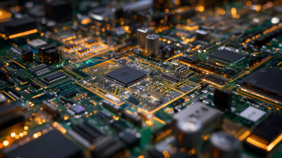
A well-designed PCB must balance component placement, routing, and thermal management. Effective component placement reduces signal interference. Ensure that high-frequency components are strategically located. Use proper spacing to avoid signal integrity issues. Signal routing should follow shortest paths without unnecessary bends. Tips for routing include using wider traces for high current and maintaining clear ground paths.
Thermal management is often overlooked. Improper heat dissipation can lead to component failure. Data suggests that nearly 25% of PCB issues arise from inadequate thermal design. To mitigate this, consider adding thermal reliefs or using heatsinks. Continuous reflection on design practices will enhance future projects. Regular reviews can help identify areas for improvement.
Key Tools and Software for Effective PCB Design
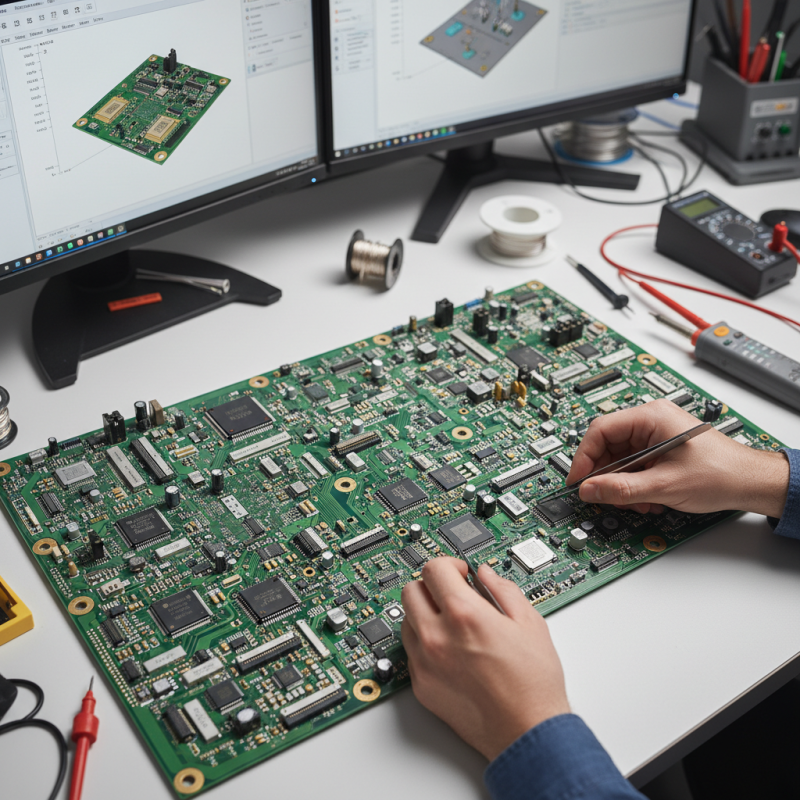
When it comes to PCB design, the right tools and software are crucial for success. Engineers often face the challenge of selecting from a multitude of options. A solid understanding of essential tools can streamline the design process.
Many users overlook the importance of simulation software. Simulation allows for testing designs before manufacturing. This can save time and costs. Consider how the design behaves under different operating conditions. It is a game-changer for identifying potential flaws upfront.
Another critical tip involves mastering layout tools. They help visualize electrical connections. Understanding how to efficiently arrange components is vital. A cluttered design often leads to errors. Take your time tackling the layout. A neat arrangement can prevent mistakes down the road.
Additionally, good collaboration software can enhance communication among team members. Working within a team often brings insights that an individual might miss. Embrace different perspectives to refine your designs further. Every detail counts, and feedback from peers can uncover hidden issues.
Essential Design Rules for Successful Circuit Layout
When designing a printed circuit board, following essential design rules is crucial. Layout complexity often leads to errors. Hence, simplifying your design is a wise move. Ensure your traces are adequately sized for current. Thin traces may overheat and fail, resulting in circuit issues.
Another key tip is to maintain proper spacing between components. Crowded designs can create unintentional short circuits. Additionally, think about grounding. A solid ground plane helps reduce noise in your circuit. If this step is overlooked, performance may suffer, affecting the entire project.
Don't forget about the orientation of your components. Aligning them neatly can save you time in troubleshooting later. Mistakes in rotation can lead to unexpected behavior. Finally, always double-check your work. A second look may catch mistakes before the manufacturing process begins. Remember, a small error can have big consequences.
10 Essential Tips for Mastering PCB Printed Circuit Board Design - Essential Design Rules for Successful Circuit Layout
| Tip Number |
Design Tip |
Description |
| 1 |
Understand Your Requirements |
Gather all specifications, including size, component types, and function. |
| 2 |
Choose the Right Materials |
Select high-quality materials that suit your design needs and environment. |
| 3 |
Optimize Component Placement |
Place components strategically to minimize trace lengths and improve signal integrity. |
| 4 |
Follow Design Guidelines |
Adhere to industry standards and best practices for PCB design. |
| 5 |
Implement Ground Planes |
Use ground planes to reduce noise and improve stability in signals. |
| 6 |
Use Correct Trace Widths |
Calculate trace widths to handle expected current loads safely. |
| 7 |
Minimize Layer Count |
Design PCBs with the least number of layers to save cost and complexity. |
| 8 |
Check for Design Rule Violations |
Run DRC checks to identify and correct any design rule issues. |
| 9 |
Plan for Thermal Management |
Incorporate thermal relief and heat dissipation strategies as needed. |
| 10 |
Test Your Design |
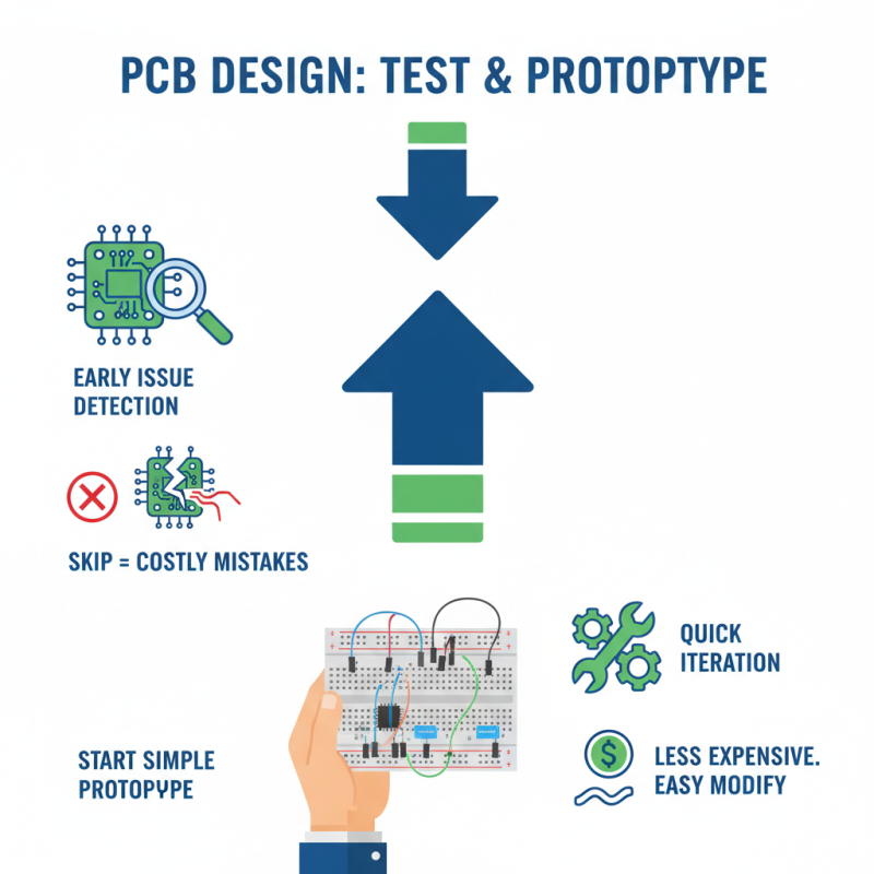
Prototype your design and conduct thorough testing before mass production. |
Techniques for Optimizing Signal Integrity in PCB Design
When designing PCBs, signal integrity is crucial. Poor signal integrity can lead to malfunctions and unreliable performance. To optimize it, start with careful trace length management. Keep traces short and direct. This minimizes resistance and inductance.
Use differential pairs for high-speed signals. They help reduce electromagnetic interference. Make sure to maintain consistent spacing. Pay attention to your ground planes. A solid ground plane can reduce noise significantly. It also helps in providing a return path for signals.
Finally, always check your design with simulations. Analyzing signals in the virtual environment can expose potential issues. But remember, simulations can’t catch everything. Even minor layout mistakes can still affect signal quality. Design requires constant learning and reflection. Keep tweaking your designs for better performance.