10 Essential Tips for Optimizing Your Circuit Board Design to Improve Performance and Reduce Costs
In the rapidly evolving field of electronics, circuit board design plays a pivotal role in determining the efficiency and cost-effectiveness of a product. Industry expert Dr. Emily Chen, a seasoned professional with over two decades of experience in PCB engineering, once remarked, "The essence of a superior circuit board design lies in the balance between performance, manufacturability, and cost." Her insight underscores the critical importance of optimizing the design process to achieve these three key objectives.
With increasing demands for high-performance and cost-effective electronic devices, engineers and designers are constantly seeking innovative strategies to enhance their circuit board designs. By incorporating essential tips into the design process, professionals can improve functionality while minimizing expenses. This article will explore ten vital strategies aimed at optimizing circuit board designs, ensuring that they meet both performance specifications and budgetary constraints.
Understanding the significance of each design tip can pave the way for developing advanced circuit boards that not only meet industry standards but also lead to competitive advantages in the marketplace. As the technology landscape continues to advance, staying informed and adaptable in circuit board design will be imperative for engineers aiming for excellence.
Best Practices for Component Placement to Enhance Signal Integrity
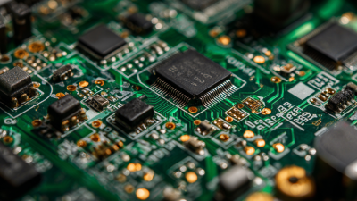
When optimizing circuit board design, effective component placement is crucial for enhancing signal integrity. According to a report from IPC, poor component layout can lead to increased electromagnetic interference (EMI), which seriously affects the performance of electronic devices. A well-planned layout minimizes loop areas and shortens signal paths, which significantly reduces noise and crosstalk. For instance, routing differential pairs in close proximity not only improves the signal's integrity but also helps maintain a consistent impedance, as highlighted in the IEEE standards for high-speed digital design.
Moreover, strategic placement of decoupling capacitors close to power pins can help stabilize voltage levels and reduce power distribution noise. A study conducted by the Institute of Engineering and Technology found that optimal placement can lower the risk of voltage drop, which is vital for maintaining performance, especially in high-frequency circuits. By adhering to these best practices, designers can not only enhance the overall functionality of their circuit boards but also mitigate potential issues that could lead to increased production costs due to rework and testing failures.
Strategies for Reducing PCB Layer Count Without Sacrificing Quality
When optimizing circuit board design, especially in the realm of medical electronics, reducing the PCB layer count without compromising quality is crucial. The complexity of compact medical devices often leads to an increased layer count due to the demand for enhanced functionality. However, by employing strategic design techniques, it's possible to achieve a more streamlined layout.
One essential tip is to implement multilayer stacking efficiently, which allows for better organization of power delivery networks and signal routing. By minimizing the number of layers needed for power and ground planes, designers can focus on essential signal traces and reduce overall complexity. Additionally, utilizing advanced materials suited for high-frequency applications, particularly in the context of 5G mmWave technologies, can help mitigate manufacturing challenges while maintaining performance.
Another strategy involves optimizing component placement to shorten trace lengths, thereby reducing parasitic capacitance and inductance, which are critical in high-speed applications. This approach not only contributes to a lower layer count but also enhances the overall signal integrity in your PCB design. By prioritizing these methods, you can effectively manage costs while ensuring that your product meets the rigorous demands of the medical electronics sector.
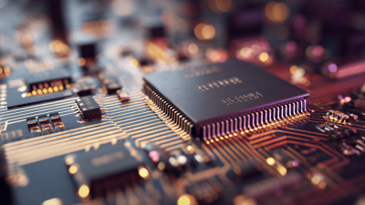
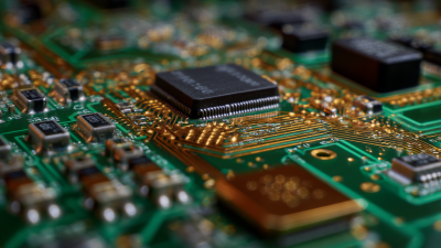
Effective Use of Via Technologies for Improved Performance
When optimizing circuit board design, the effective use of
via technologies plays a crucial role in enhancing performance
while simultaneously reducing costs. Vias serve as the connection points between different layers of a
printed circuit board (PCB), and their strategic
placement can significantly impact signal integrity and electronic performance. By utilizing blind and buried vias,
designers can create compact layouts that minimize the trace lengths, thus reducing
inductance and capacitance,
which ultimately leads to improved signal quality.
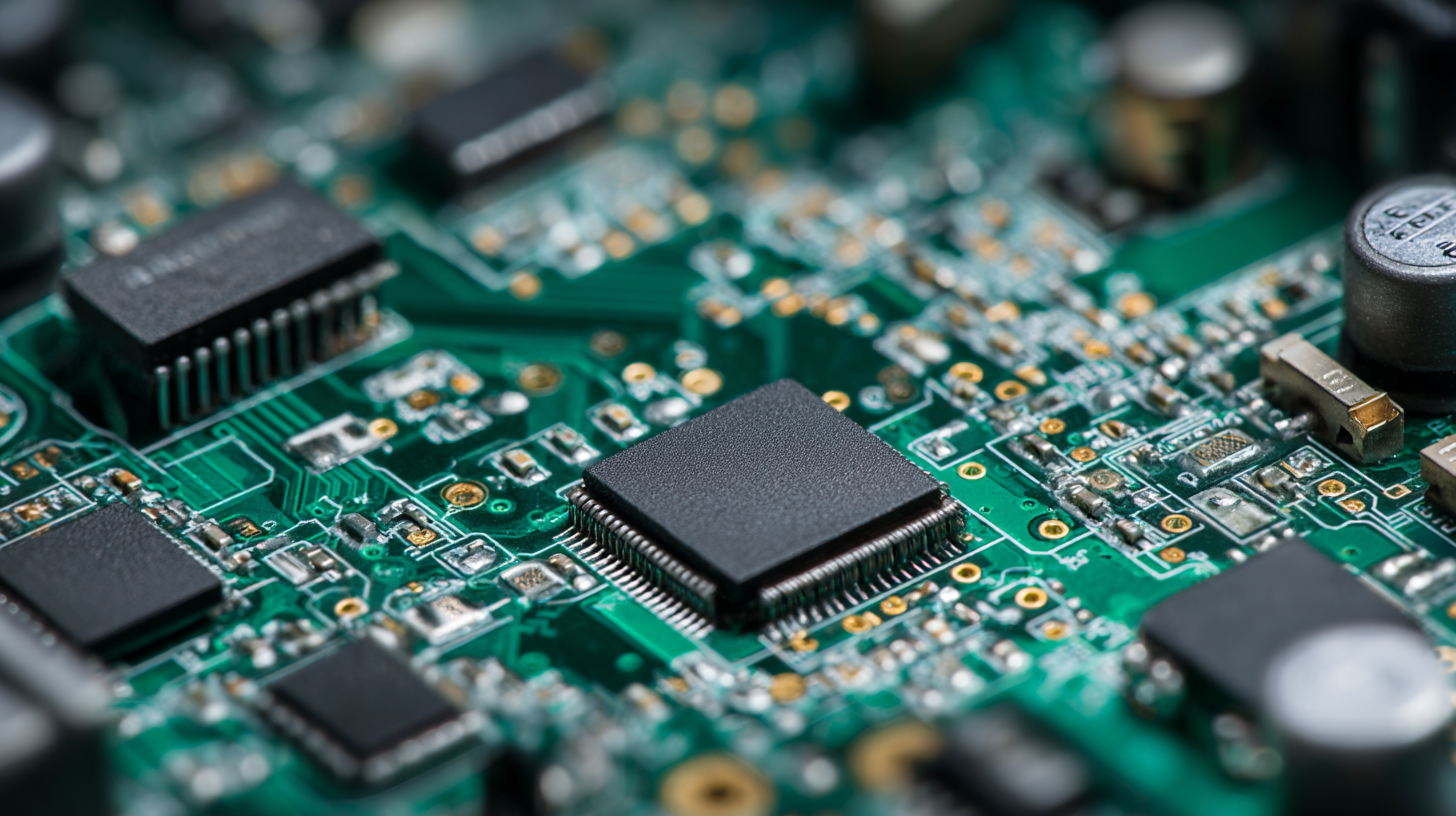
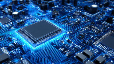
Additionally, the choice between microvias and
traditional vias can further optimize the design. Microvias, typically used in high-density interconnect (HDI) boards, allow for tighter routing and can
accommodate more complex circuitry within a smaller footprint. This not only enhances performance by improving
signal speed and reliability but also contributes to cost savings by reducing material usage and the overall
size of the board. Implementing via-in-pad technology can also help
in managing thermal and electrical performance, making it easier to dissipate heat and ensuring that the board
operates efficiently within its intended environment.
Thermal Management Techniques to Optimize Circuit Board Efficiency
Effective thermal management is a critical component in optimizing circuit board performance and reducing costs. Recent advancements highlight the use of 2D hexagonal boron nitride (hBN) coatings, which significantly enhance heat dissipation in electronic devices. This innovative approach not only improves the thermal efficiency of circuit boards but also contributes to reducing power consumption, making it a cost-effective solution for manufacturers. As evidenced by research, implementing cooling technologies can lead to a notable increase in component reliability and overall performance, particularly in high-demand sectors such as AI and cloud computing.
To further optimize circuit board designs, consider the following essential tips: Firstly, integrating thermal gap fillers can effectively manage heat transfer while minimizing stress and deflection in PCB assemblies. These materials ensure efficient thermal conduction and can sustain the structural integrity of the boards. Secondly, using advanced packaging techniques that enhance airflow around components will improve heat dissipation, subsequently prolonging the lifespan of the electronic assemblies. Additionally, conducting a thorough analysis of thermal design power (TDP) requirements can guide the selection of suitable materials and layouts, enabling designers to strike a balance between performance and cost, thus leading to innovations in high-speed interface designs.
Cost-Effective Material Choices for High-Performance Circuit Boards
When designing high-performance circuit boards, selecting cost-effective materials is paramount for balancing performance and budget. An industry report by IPC indicated that nearly 70% of a PCB's manufacturing cost is attributed to material selection. Therefore, choosing materials that offer both affordability and functionality can lead to significant savings without compromising on quality. Materials like FR-4, a standard base material for PCBs, present a practical solution due to their low cost and adequate performance in moderate application environments.
Advancements in material science also provide alternatives that can enhance performance while keeping costs down. For example, polyimide flex circuits offer excellent thermal stability and electrical properties at a competitive price point, making them suitable for high-temperature applications. Additionally, reports suggest that using embedded passive components within circuit boards can minimize space and cost, streamlining production while enhancing performance. By leveraging these innovative materials, engineers can optimize circuit board designs to achieve desired performance metrics while adhering to budgetary constraints.