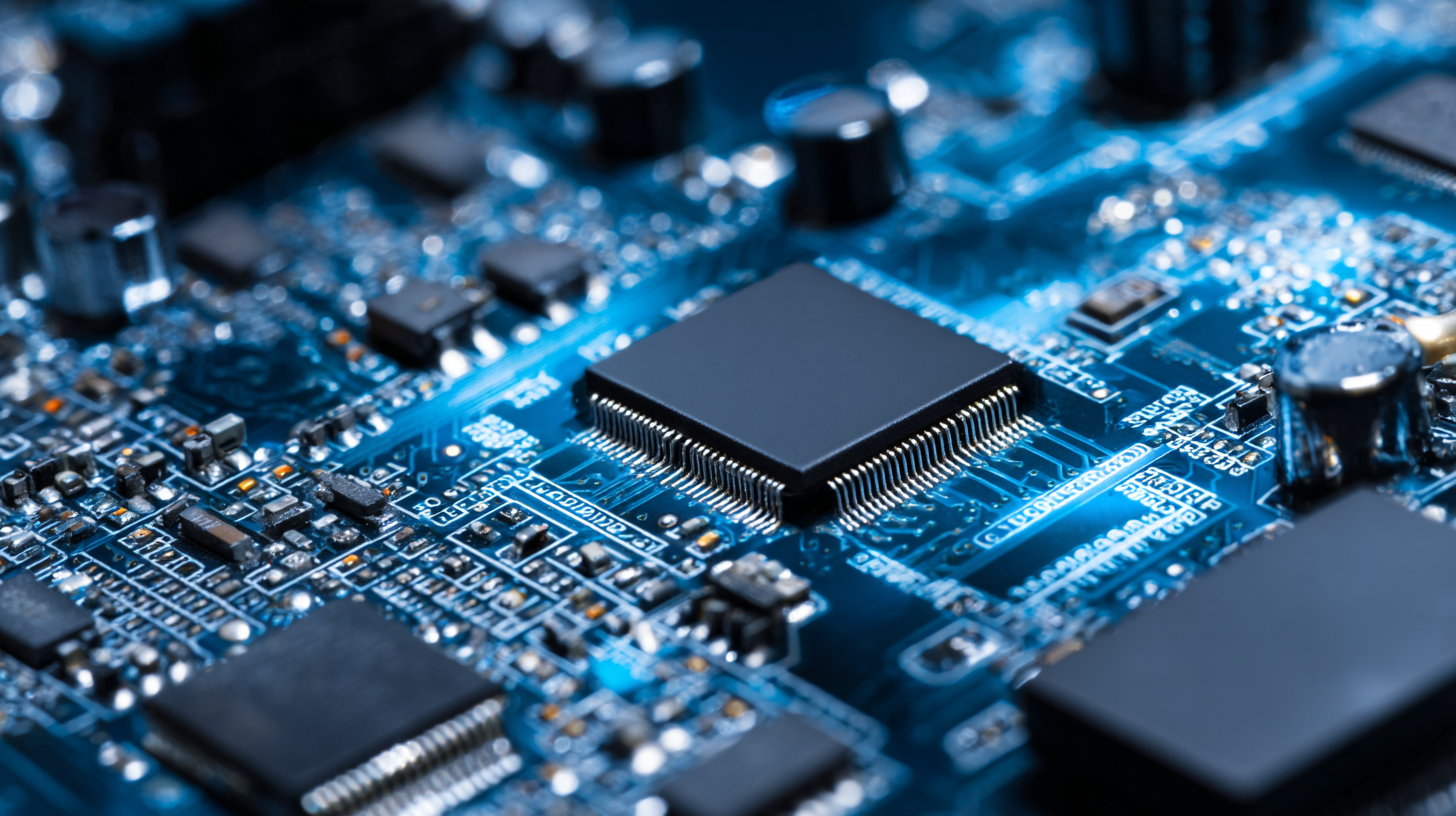
Exploring the Future of PCB Board Manufacturing: Innovations Leading the Way
The landscape of pcb board manufacturing is undergoing significant transformation driven by innovative technologies and methodologies that promise to enhance efficiency, reduce costs, and improve product quality. According to a recent report by Research and Markets, the global printed circuit board market is projected to reach approximately $85 billion by 2025, with a compound annual growth rate (CAGR) of around 3.5% from 2020 to 2025. This growth is largely fueled by the increasing demand for advanced consumer electronics, automotive applications, and emerging technologies such as 5G, IoT, and AI. As manufacturers explore cutting-edge approaches, including automation, additive manufacturing, and smart technologies, the pcb board manufacturing sector stands on the brink of a technological revolution that could redefine industry standards and pave the way for a more sustainable and efficient future.
Understanding the Basics of PCB Board Manufacturing Processes
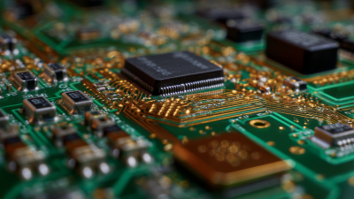
The manufacturing process of Printed Circuit Boards (PCBs) is a complex and meticulous endeavor that serves as the backbone of modern electronics. At its core, PCB manufacturing begins with design and layout, where engineers utilize sophisticated software to create intricate schematics that define the circuit paths. This digital blueprint is then translated into physical form via various processes, such as photolithography, etching, and layering, which involve applying photoresist, exposing it to light, and chemically removing unwanted copper to form conductive pathways.
After achieving the desired circuitry, the next essential step is assembling the components onto the PCB. This is often done through surface mount technology (SMT) or through-hole methods. Each component is carefully placed and soldered, ensuring electrical connections are secure for optimal performance. Additionally, advancements in automation and robotics are enhancing efficiency and precision in the assembly process, paving the way for faster production times and improved quality control. As these foundational processes evolve, they set the stage for future innovations in PCB manufacturing, ultimately driving the electronics industry's growth.
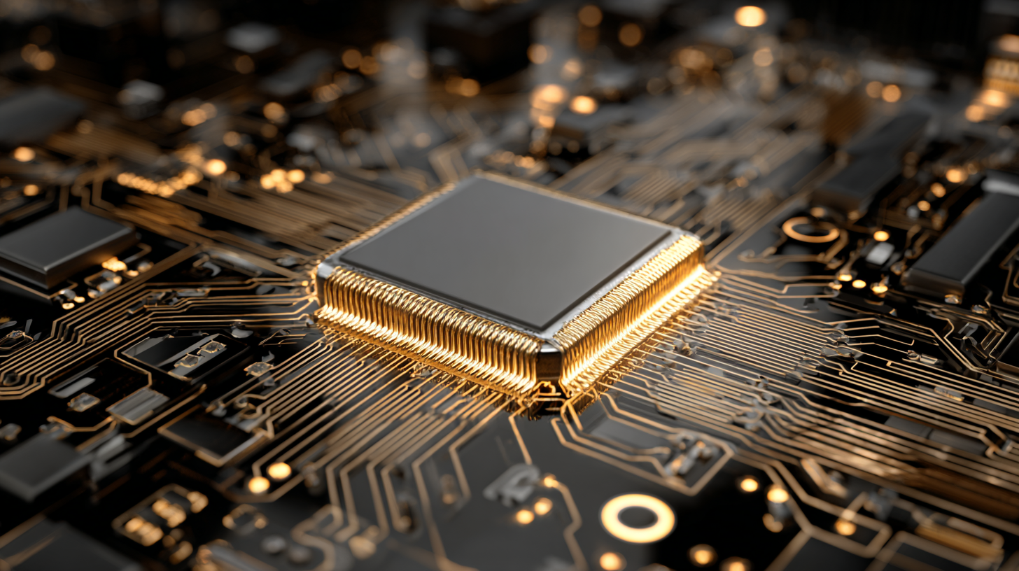
Identifying Key Innovations Transforming PCB Production
The future of PCB (Printed Circuit Board) manufacturing is being reshaped by a range of innovative technologies that are streamlining production processes and enhancing product performance. Key advancements include the adoption of advanced materials such as flexible substrates and high-frequency laminates. These materials not only improve the durability and performance of PCBs but also enable the design of more compact and efficient electronic devices.
Tips: When considering materials for PCB production, assess the specific requirements of your application. For high-frequency circuits, prioritizing materials with low dielectric loss can significantly impact signal integrity.
Another transformative innovation is the integration of
automation and
AI-driven systems in the manufacturing process. Automated inspection systems and robotic assembly lines reduce human error and speed up production time, allowing for quicker iterations and more complex designs. Manufacturers who invest in these technologies can gain a competitive edge in a rapidly evolving market.
Tips: Implementing AI solutions can help optimize your production schedules and manage inventory more effectively. Regularly evaluate and update your automation processes to keep pace with industry advancements.
Evaluating the Role of Automation in Future PCB Manufacturing
The evolution of PCB board manufacturing is increasingly intertwined with advancements in automation. Automation technologies such as robotics and artificial intelligence are transforming traditional manufacturing processes, enhancing efficiency, and improving production quality. These technologies enable manufacturers to streamline operations, reduce human error, and create highly precise circuit boards at a faster rate. By implementing automated systems, manufacturers can better manage complex designs and intricate layouts that modern electronics demand.
Moreover, automation provides valuable data analytics capabilities that contribute to continuous improvement. Integrated sensors and monitoring systems offer real-time insights into the manufacturing process, allowing for proactive adjustments and predictive maintenance. This data-driven approach not only helps in minimizing downtime and waste but also ensures that the final products meet the highest standards of reliability and performance. As PCB manufacturing continues to advance, the role of automation will be pivotal in meeting the growing demands of the electronics market and pushing the boundaries of innovation.
Exploring Sustainable Practices in PCB Production Technology
Sustainable practices in PCB production technology are increasingly vital as the electronics industry faces growing pressure to minimize its environmental footprint. Manufacturers are exploring non-toxic materials, such as bio-based resins and lead-free solder, to replace traditional harmful substances. These innovations not only help in reducing waste and pollution but also enhance the durability and efficiency of the printed circuit boards. The transition to renewable energy sources in manufacturing processes further contributes to a greener production environment.
Tips for manufacturers looking to adopt sustainable practices include: first, invest in research and development to find alternative materials that meet industry standards while being environmentally friendly. Second, implement a closed-loop recycling system to reduce waste and recover valuable metals and components. Lastly, engage with supply chain partners who prioritize sustainability, fostering a collaborative approach to environmentally responsible manufacturing.
Moreover, the integration of smart technology in production lines offers the potential for better resource management. By using IoT sensors and data analytics, manufacturers can optimize energy consumption and effectively track material usage, leading to lower operational costs and a reduced carbon footprint. Embracing these sustainable practices not only meets regulatory demands but also positions manufacturers as leaders in an evolving market that values eco-friendly solutions.
Exploring Innovations in PCB Board Manufacturing
Adopting Advanced Materials for Enhanced PCB Performance
The demand for high-performance printed circuit boards (PCBs) is driving innovations in the use of advanced materials within the industry. A recent report by MarketsandMarkets forecasts that the global PCB market will reach $78.6 billion by 2027, growing at a CAGR of 4.1%. This growth is partly attributed to the increasing need for lightweight and durable materials that can sustain high-frequency applications, especially in sectors such as telecommunications and automotive. Materials such as polyimide, liquid crystal polymer (LCP), and ceramic-filled resins are gaining traction due to their superior thermal stability and dielectric properties, which significantly enhance the overall performance of PCBs.
In addition to optimizing performance, the adoption of advanced materials is also being driven by the push for greener manufacturing processes. The IPC's 2022 report highlights that eco-friendly PCB materials, including bio-based substrates and lead-free solder, are becoming increasingly favored, helping companies meet regulatory requirements and consumer demand for sustainable practices. Furthermore, integrating these innovative materials can lead to reductions in weight and material waste, ultimately resulting in cost savings and improved reliability in electronic devices. As manufacturers continue to explore these advanced options, the landscape of PCB fabrication is undoubtedly set for a transformative shift.
Exploring the Future of PCB Board Manufacturing: Innovations Leading the Way - Adopting Advanced Materials for Enhanced PCB Performance
| Material |
Thermal Conductivity (W/mK) |
Dielectric Strength (kV/mm) |
Flexibility (Bending Radius) |
Applications |
| High-Tg FR-4 |
0.45 |
20 |
8 mm |
Consumer Electronics |
| Polyimide |
0.25 |
15 |
2 mm |
Aerospace |
| Ceramic |
1.0 |
30 |
5 mm |
High-Power Applications |
| Metal Core PCB |
1.5 |
25 |
6 mm |
LED Lighting |
| Rigid-Flex |
0.30 |
18 |
4 mm |
Medical Devices |