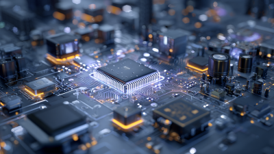
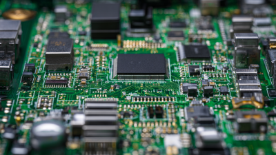
Understanding the Latest Trends in PCB Circuit Board Technology for Efficient Design
In today's rapidly evolving electronics industry, understanding the latest trends in
PCB circuit board technology is crucial for achieving efficient design and production processes.
According to a report by MarketsandMarkets, the global PCB market is expected to reach USD 82.2 billion by 2026, driven by the
rising demand for electronic devices across various sectors, including automotive, healthcare, and telecommunications.
Recent advancements in materials, such as the use of high-frequency substrates and eco-friendly laminates, are redefining
the capabilities of PCB circuit boards, allowing for higher performance and sustainability.
Furthermore, the integration of smart technologies, such as IoT and AI, is paving the way for more
innovative and compact designs that enhance functionality while reducing manufacturing costs.
This article will explore key trends and best practices in PCB circuit board design, providing insights to help engineers stay ahead in a
competitive landscape.
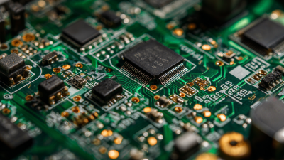
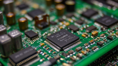
Emerging Technologies in PCB Design and Manufacturing
The landscape of PCB design and manufacturing is rapidly evolving, propelled by emerging technologies that are reshaping how electronic circuits are developed. According to a recent report from Research and Markets, the global PCB market is projected to reach $81.21 billion by 2026, growing at a CAGR of 4.87%. This growth is largely driven by advances in automation and the integration of smart technologies, which are enhancing production efficiency and reducing time-to-market for new products.
One of the most significant trends in PCB design is the adoption of high-density interconnect (HDI) technology. As devices become more compact, incorporating HDI allows for greater functionality in smaller form factors, thus meeting the demands of Industries such as consumer electronics and telecommunications. Additionally, the rise of Internet of Things (IoT) applications is pushing designers to explore new materials and techniques, such as flexible PCBs, which enable innovative product designs that are both lightweight and durable. A market analysis by Mordor Intelligence highlights that the flexible printed circuit segment is expected to grow significantly, with a projected CAGR of 11.15% from 2021 to 2026, underscoring the importance of adaptability in future PCB solutions.
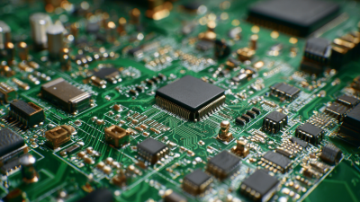
Sustainable Practices in Circuit Board Production
As the demand for more efficient and environmentally friendly manufacturing processes increases, sustainable practices in circuit board production are becoming more crucial. One key trend is the use of eco-friendly materials that reduce the environmental impact of PCB fabrication. Manufacturers are increasingly opting for materials that are non-toxic and recyclable, ensuring that the lifecycle of the circuit board is more sustainable.
Tips: Consider using biodegradable substrates or halogen-free laminates in your designs. This not only enhances your product's sustainability but also appeals to an environmentally conscious market.
Another significant trend is the implementation of energy-efficient manufacturing techniques. Utilizing advanced manufacturing technologies, such as additive manufacturing and automation, can significantly reduce energy consumption. These approaches not only minimize waste but also lead to faster production times.
Tips: Evaluate the energy consumption of your production processes regularly. Implementing energy-efficient machinery and optimizing workflow can lead to significant cost savings and a reduced carbon footprint.
Incorporating these sustainable practices not only benefits the environment but also enhances the credibility of your brand in a competitive market. By prioritizing sustainability in PCB production, companies can align themselves with global efforts towards a greener future.
The Role of AI and Automation in PCB Development
The advent of artificial intelligence (AI) and automation in PCB (Printed Circuit Board) development has revolutionized the way designers approach circuit board design and manufacturing. AI tools now facilitate advanced simulations and optimizations, enabling engineers to predict performance issues and identify design flaws early in the development process. This proactive approach not only reduces the time spent on debugging and revisions but also enhances the overall reliability of the final product.
Automation also plays a crucial role in streamlining PCB assembly and testing processes. Automated systems can handle repetitive tasks with precision, thereby increasing production efficiency and reducing labor costs. Additionally, automated inspection technologies equipped with AI algorithms can detect defects that may be missed by human operators, ensuring the highest quality standards are maintained. Together, AI and automation not only foster innovation in PCB design but also significantly contribute to efficient manufacturing processes, thus meeting the rising demand for more complex and miniaturized electronic devices.
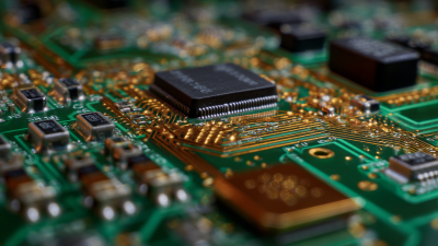
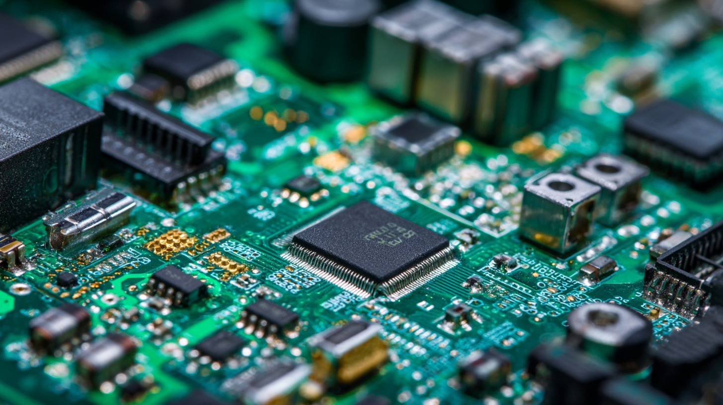
Trends in High-Speed PCB Materials and Components
In the rapidly evolving landscape of electronics manufacturing, high-speed PCB materials and components have taken center stage. The push for efficiency and performance in circuit board designs underscores the critical role that advanced materials play in enhancing signal integrity and reducing latency. Innovations such as low-loss laminates and advanced copper plating techniques are setting new benchmarks for speed and reliability. As manufacturers seek to accommodate faster data rates and increasing complexities in electronic devices, the adoption of these cutting-edge materials becomes essential.
Simultaneously, the rise of startups in the field reflects a burgeoning ecosystem focused on technological advancements. Out of thousands of new ventures, twenty standout companies are making waves by introducing pioneering solutions that streamline manufacturing processes and improve product functionality. These startups are harnessing trends such as automation, AI integration, and sustainable practices to reshape the electronics landscape. Their impact cannot be overstated, as they not only enhance design capabilities but also drive down costs and accelerate time-to-market for new innovations. This vibrant environment of high-speed PCB materials and component trends is set to redefine the future of electronics design and manufacturing.
Integrating IoT with PCB Design for Smart Electronics
The integration of Internet of Things (IoT) technology with PCB design is transforming the landscape of smart electronics, driving innovation and efficiency in product development. According to a recent report by Markets and Markets, the global IoT market is projected to grow from $150 billion in 2021 to over $1 trillion by 2026, indicating a significant demand for advanced PCB technologies that support these systems. Modern PCBs are becoming increasingly complex, requiring sophisticated design methodologies to accommodate wireless connectivity, sensors, and microcontrollers that are integral to IoT devices.
One key trend in PCB design is the shift towards multi-layered boards that enhance functionality while minimizing space. As per a TechNavio report, over 48% of smart device manufacturers are investing in advanced multi-layer PCB technology to meet the demands of compact designs. This development not only allows for the incorporation of more components in a smaller area but also enhances signal integrity and reduces electromagnetic interference, which are critical for reliable IoT performance. Additionally, the adoption of flexible and rigid-flex PCBs supports diverse applications ranging from wearable technology to industrial IoT systems, further underscoring the pivotal role of PCB innovation in the ongoing IoT revolution.
Understanding the Latest Trends in PCB Circuit Board Technology for Efficient Design - Integrating IoT with PCB Design for Smart Electronics
| Trend |
Description |
Impact on Design |
Integration with IoT |
| Flex PCB Technology |
Flexible PCBs enable designs that can bend and twist, allowing for innovative product shapes. |
Improves space utilization and reduces weight in electronic devices. |
Enhances compact sensor deployment in IoT devices. |
| High-Frequency PCB Materials |
Materials engineered for high-frequency applications, ensuring signal integrity. |
Supports reliable data transmission for high-speed applications. |
Critical for IoT devices that require fast and reliable connectivity. |
| Embedded Components |
Integration of components directly into the PCB to improve design efficiency. |
Reduces PCB size and assembly time. |
Facilitates the miniaturization of IoT devices. |
| Advanced Soldering Techniques |
Techniques such as laser soldering reduce thermal stress on sensitive components. |
Increases reliability of assembly for delicate electronics. |
Ensures secure connections in remote IoT devices. |
| Green PCB Manufacturing |
Sustainable practices in PCB production, focusing on environmental impact. |
Meets regulations while appealing to eco-conscious consumers. |
Supports circular economy initiatives in IoT device lifecycle management. |