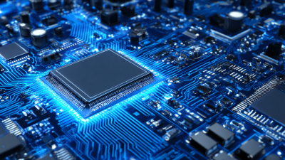
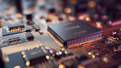
What is a PCB Board and Why is it Important in Electronics?
In the world of electronics, the PCB board stands as a fundamental building block. Experts agree on its significance. Dr. Emily Chen, a leading authority in electronic engineering, emphasizes, "A PCB board is the lifeline of all electronic devices." This statement highlights the board's role in connecting components and ensuring functionality.
PCBs are present in almost every gadget we use. From smartphones to home appliances, they facilitate the communication between various parts. However, many overlook their complexities. The design and material choices can affect performance dramatically. A poorly designed PCB can lead to device failure, which is a critical concern in development.
Yet, as technology evolves, the demands on PCB boards increase. Innovators must constantly refine their designs to keep up. The challenges are real, and reflection on these obstacles is essential for progress. Balancing cost, design, and function remains an ongoing struggle in the industry. The future of electronics hinges on the evolution of the PCB board.
Understanding the Basics of PCB Boards in Electronics
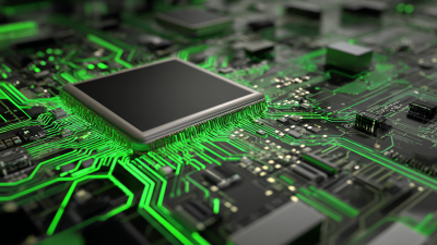
PCB boards, or printed circuit boards, are essential components in modern electronics. They serve as the backbone of electronic devices, connecting different components like resistors, capacitors, and microchips. The board itself is made of non-conductive material, usually coated with a conductive pathway. This pathway guides electrical signals and power, ensuring that the device functions as intended.
Understanding PCB boards involves recognizing their various types. Single-layer PCBs are simple and common, while multi-layer boards offer intricate connections for more complex devices. The design of these boards can be quite complicated. Mistakes in design can lead to device failure. This happens when the pathways are incorrectly laid out or components are not positioned properly. Testing is crucial but not always foolproof. Even small errors can have significant consequences.
Importance of PCB Boards in Electronics
This bar chart illustrates the key advantages of using PCB (Printed Circuit Board) in electronic devices, highlighting how various factors contribute to their significance in modern electronics.
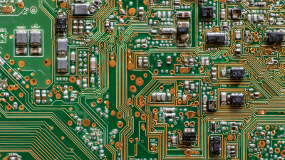
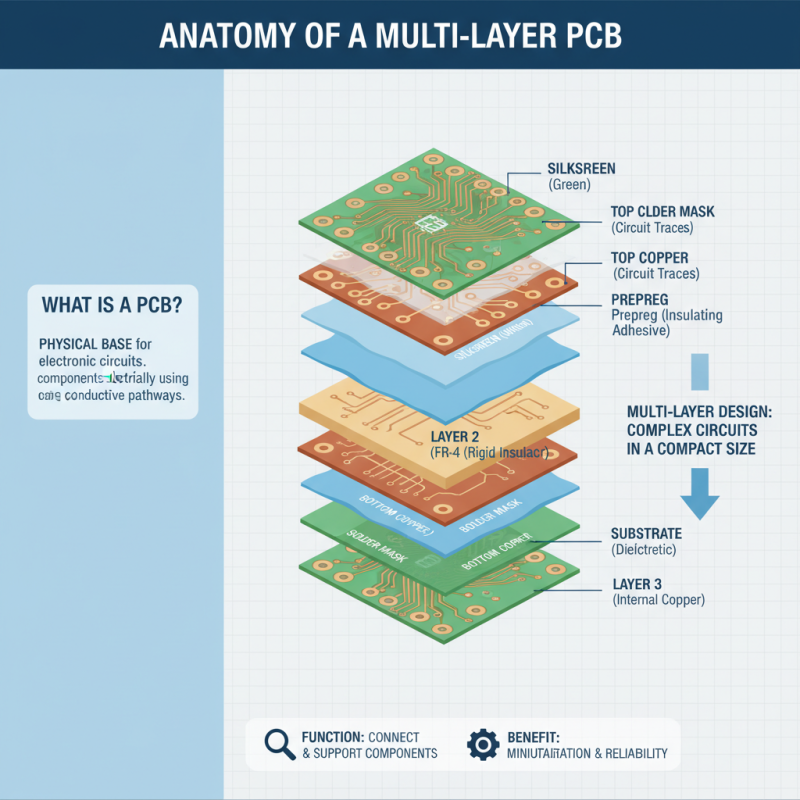
The Structure and Components of a PCB Board
A PCB board, or printed circuit board, is a fundamental component in electronics. It provides the physical base for electronic circuits. The structure typically consists of several layers, with a common configuration being a multilayer board. This design allows for more complex circuitry without increasing the board's physical size.
PCB boards consist of several essential components. The base material, usually fiberglass, provides strength and insulation. Conductive traces, made from copper, connect different components. These connections form the electrical pathways for signals. According to industry reports, the PCB market is projected to reach $78 billion by 2025, indicating growing demand for these boards.
Despite their importance, not all PCBs are created equally. Poor design can lead to malfunction or signal integrity issues. The thickness of the copper layer and the quality of the solder mask are often overlooked, resulting in failure during production. Continuous improvements in technology drive better manufacturing practices, but inconsistencies still arise. Thus, understanding the structure and quality of PCB components is essential for reliable electronics.
The Manufacturing Process of PCB Boards
The manufacturing process of PCB boards involves several critical steps that ensure quality and reliability. A notable report from IPC indicates that the global PCB market surpasses $60 billion annually. This demand emphasizes the significance of precision in each manufacturing phase.
Initially, copper layers are laminated onto a substrate. This forms the base where circuits will be etched. Chemicals used during etching must be carefully managed to minimize waste. It's noted that up to 15% of materials can be lost if not properly handled. After etching, the layers are drilled for holes. Precision is vital here; a 0.1 mm error can render the board unusable.
Surface finish is crucial for solderability and longevity. Various techniques like hot air leveling are employed. However, inconsistent quality can occur, and around 5% of boards fail inspection due to surface defects. Finally, thorough testing follows, ensuring electrical properties meet standards. Despite advancements, challenges remain. The need for sustainable practices in material sourcing is increasingly urgent. Balancing quality and eco-friendliness is a pressing issue for manufacturers.
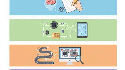
Applications and Significance of PCBs in Modern Devices
Printed Circuit Boards (PCBs) are at the heart of modern electronics. Their significance is towering. According to a recent industry report by Mordor Intelligence, the global PCB market is projected to reach USD 80 billion by 2026. This reflects an annual growth rate of 4% from 2021. Consumers require compact devices with higher performance, pushing for innovative PCB designs. The shift towards miniaturization leads to sophisticated applications in smartphones, computers, and medical devices.
The implications of PCB usage extend beyond consumer electronics. Automotive applications are increasingly reliant on advanced PCBs. A report by Research and Markets forecasts the automotive PCB sector to see growth due to electric vehicles. In fact, nearly 30% of a modern electric vehicle's cost is attributed to electronics. This increase reveals a pressing need for efficient and flexible PCB manufacturing processes. However, the industry still faces challenges, such as the recycling of PCBs to tackle e-waste. Solutions for sustainability are often lagging behind technological advancements. This gap necessitates ongoing dialogue and innovation in PCB design and production.
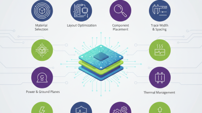
Challenges and Innovations in PCB Design and Production
The landscape of PCB design and production faces myriad challenges. One major issue is the increasing complexity of electronic devices. As devices become more compact, PCBs must accommodate intricate layouts. A report from IPC indicates that nearly 70% of designers struggle with space constraints.
Additionally, environmental regulations push for greener materials and processes. This shift complicates production, as manufacturers must innovate without sacrificing performance. According to a recent survey, about 55% of PCB producers recognize compliance as a growing challenge. The integration of sustainable practices can generate waste and disrupt established workflows.
Despite these challenges, innovation thrives. Technologies like additive manufacturing are reshaping how PCBs are produced. This method allows for rapid prototyping and better material efficiency. Over 40% of industry experts believe that adopting advanced technologies will be crucial for staying competitive. Yet, as exciting as these trends are, they require continuous learning. Many engineers find themselves overwhelmed by the pace of change in materials and methods.