How to Design PCB for Beginners and Advanced Users?
Designing PCB is both an art and a science. Many beginners feel overwhelmed. However, with the right guidance, anyone can learn to design PCB effectively. Renowned expert Dr. Emily Chen states, "The key to mastering PCB design is understanding the basics first." Her advice is invaluable for novices.
For beginners, the process starts with simple tools and techniques. It's essential to grasp the fundamentals before diving into complex layouts. Understanding how components fit together physically and electrically is crucial. Even advanced users must revisit these basics periodically for growth.
As one navigates through PCB design, challenges will arise. Mistakes are common, but they can serve as powerful learning experiences. Reflecting on these errors encourages improvement. The journey to design PCB is filled with ups and downs, but each step fosters knowledge and skill. Embrace the process, and don't hesitate to seek help from experienced designers.
Understanding the Basics of PCB Design for Beginners
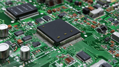
Understanding the basics of PCB design is essential for both beginners and advanced users. Printed Circuit Boards (PCBs) serve as the backbone of electronic devices. According to a report from IPC, the global PCB market is expected to reach $75 billion by 2025, highlighting its importance in modern electronics.
For beginners, starting with simple software tools can be beneficial. Tools like Fritzing or EasyEDA offer user-friendly interfaces. Yet, many beginners overlook the importance of trace width calculations. This error can lead to overheating or even circuit failure. Understanding current-carrying capacity is crucial. Surprisingly, up to 30% of novice designs encounter issues due to inadequate trace widths.
Designing a PCB requires attention to component placement too. Beginners often crowd components, making soldering difficult. A well-thought-out layout enhances manufacturability and reliability. Many professionals suggest leaving at least 0.25 inches between components. Also, using ground planes improves performance. Yet, advanced users sometimes dismiss this, leading to noise issues in high-frequency designs. Reflecting on these aspects can refine both designs and problem-solving skills.
PCB Design Skill Levels Among Users
Key Tools and Software for PCB Design
When it comes to PCB design, selecting the right tools is crucial. A 2022 report by Statista highlighted that the global PCB CAD software market is projected to reach $1.2 billion by 2026. This growth emphasizes the importance of effective design tools.
For beginners, user-friendly software like Fritzing or KiCad can simplify the learning curve. They offer intuitive interfaces and essential features for basic PCB layouts.
Advanced users may require more robust solutions, such as Altium Designer or Eagle. These tools provide advanced simulation capabilities and enhanced layout features. A study from IPC revealed that 75% of engineers prefer software that integrates simulation and design functionalities seamlessly. This integration can significantly reduce design errors, boosting reliability.
Despite the advances in software, challenges remain. Users often encounter limitations with free versions, like restricted layer counts or fewer component libraries. These constraints can hinder complex projects. Additionally, many software require a steep learning curve. This can discourage new designers from fully exploring their potential.
Focusing on the right tools can enhance both the design experience and the final product's quality.
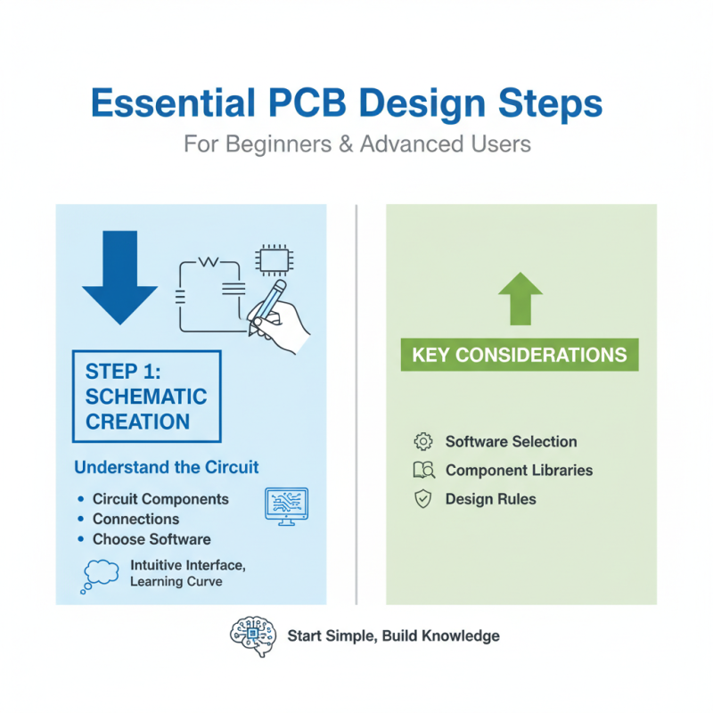
Essential PCB Design Steps for Beginners and Advanced Users
When designing a PCB, beginners should start with a clear understanding of the essential steps involved. The first task is schematic creation. This requires knowing the circuit components and their connections. It's crucial to choose the right software for this step. Many programs offer intuitive interfaces, making it easier for beginners. But remember, the learning curve can be steep.
Next, layout design follows. Beginners often overlook space optimization, leading to component crowding. Proper placement ensures better functionality. Even advanced users might face challenges here. They need to adhere to design rules while incorporating their unique ideas. Test points should be included for future troubleshooting, but these details can be missed initially.
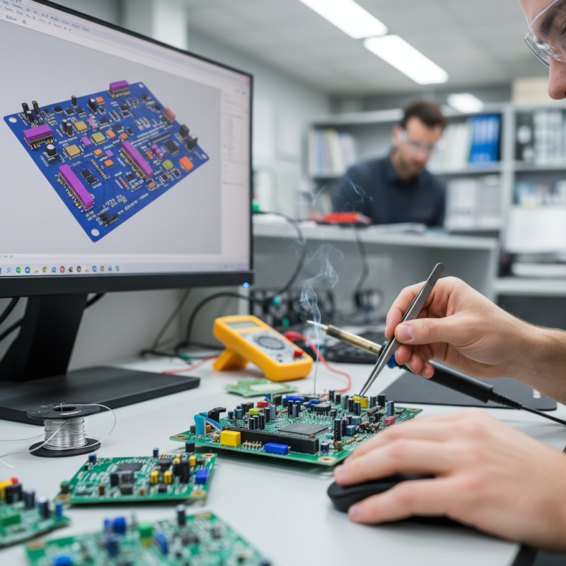
For both beginners and advanced users, reviewing the design is key. Errors can slip through the cracks. A fresh pair of eyes may spot issues that you missed. Always run simulations before finalizing your design. This process can reveal unexpected problems. Learning from mistakes is vital in PCB design, creating a cycle of continuous improvement.
Common Mistakes in PCB Design and How to Avoid Them
Designing printed circuit boards (PCBs) requires careful attention to avoid common pitfalls. Many beginners overlook clearance requirements. This oversight can lead to short circuits. According to a report by IPC, nearly 40% of PCB failures stem from inadequate spacing. Always ensure there's sufficient gap between traces, especially in high-voltage applications.
Another frequent mistake is ignoring the thermal management of the design. Components can heat up quickly, causing damage. A study from TechInsights revealed that overheating is responsible for over 25% of electronic failures. Utilize thermal vias and heatsinks for effective heat dissipation. Keep track of component temperatures throughout the design phase.
**Tip:** Consider using simulation software to visualize thermal performance before finalizing your layout.
Inadequate grounding is also a critical issue. Poor grounding can lead to signal integrity problems and electromagnetic interference. A reliable grounding strategy minimizes noise and improves performance. A research paper from the IEEE found that optimizing ground planes can reduce interference by up to 50%.
**Tip:** Use a star grounding technique to minimize interference among components.
Reflecting on your design decisions is crucial. Being mindful of these common mistakes can enhance the reliability of your PCB designs. Prioritizing thorough reviews helps to prevent these pitfalls in both beginner and advanced projects.
How to Design PCB for Beginners and Advanced Users? - Common Mistakes in PCB Design and How to Avoid Them
| Mistake |
Description |
Solution |
| Ignoring Manufacturer Guidelines |
Designing without adhering to the PCB manufacturer's specifications. |
Always consult the manufacturer’s guidelines and design rules before starting. |
| Poor Component Placement |
Components placed too close can cause interference and signal integrity issues. |
Plan your layout to keep components appropriately spaced based on their function. |
| Not Using a Ground Plane |
Failing to implement a ground plane can lead to noise and electromagnetic interference. |
Include a solid ground plane to minimize noise and enhance performance. |
| Inadequate Testing Points |
Not providing enough test pads or points can make debugging difficult. |
Integrate ample testing points for easier inspections and troubleshooting. |
| Ignoring Thermal Management |
Failure to manage heat can lead to component failure. |
Consider using heat sinks and ensure proper airflow in your design. |
Advanced Techniques for Optimizing PCB Layout and Performance
When designing printed circuit boards (PCBs), advanced techniques can significantly impact layout efficiency and performance. One common approach is impedance matching. This technique ensures that signals travel with minimal reflection. A report from IPC indicates that proper impedance control can improve signal integrity by up to 90%. Successful implementation often requires careful consideration of trace width and spacing.
Another vital technique is optimizing layer stack-up. A balanced stack-up enhances electromagnetic compatibility (EMC) and minimizes crosstalk. According to recent industry studies, PCBs with a well-optimized layer structure can reduce noise levels by 30%. Designers should evaluate their materials, considering dielectric constants that align with their project needs. However, miscalculating layer arrangements can lead to unexpected performance issues.
Thermal management is also critical in advanced PCB design. Elevated temperatures can decrease lifespan and performance. Advanced thermal simulation tools allow engineers to predict heat dissipation. Reports suggest that integrating proper thermal vias can lower critical component temperatures by as much as 25%. Yet, over-reliance on simulations may lead to complacency, making real-world testing crucial.