What is PCB Fabrication and Assembly Process Explained?
The world of PCB fabrication and assembly is intricate and fascinating. Experts like Dr. Emily Tran emphasize its significance: "The quality of PCB fabrication and assembly directly impacts device performance." Understanding this process is critical for engineers and manufacturers alike.
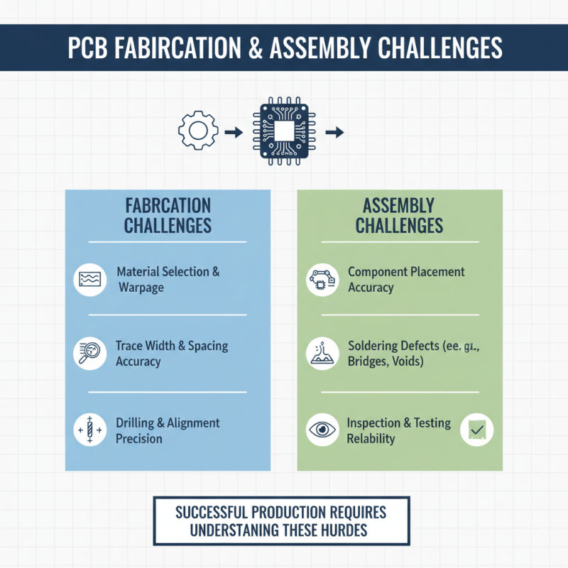
In PCB fabrication, raw materials undergo several complex processes. Techniques such as etching and layering transform simple substrates into functional circuits. Assembly involves placing components accurately. This requires precision and skill. Yet, the reality often shows discrepancies in execution. Mistakes can lead to functional failures.
Looking closely, the industry faces challenges, like ensuring consistent quality. Variations in techniques affect outcomes. This calls for constant reflection and improvement on best practices. The road to mastery in PCB fabrication and assembly is long, requiring ongoing adaptation and learning.
Overview of PCB Fabrication and Assembly Process
The PCB fabrication and assembly process is essential in electronic manufacturing. It begins with design, where engineers create circuit layouts. These layouts are then translated into physical boards, known as PCBs. A good PCB design is critical; errors can lead to costly reworks.
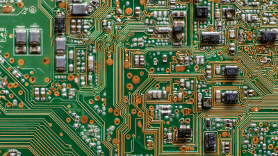
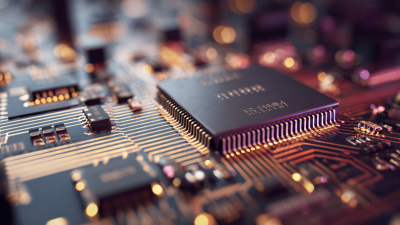
Next, various materials are used to create the PCB. Copper, for instance, is used for traces. Layers are built up through etching, drilling, and lamination. Each step requires precision, as minor mistakes can affect the board's functionality.
Tips: Always double-check your design files. Mistakes in the design can result in wasted materials and time. Pay attention to the layout; it will impact how components fit together later.
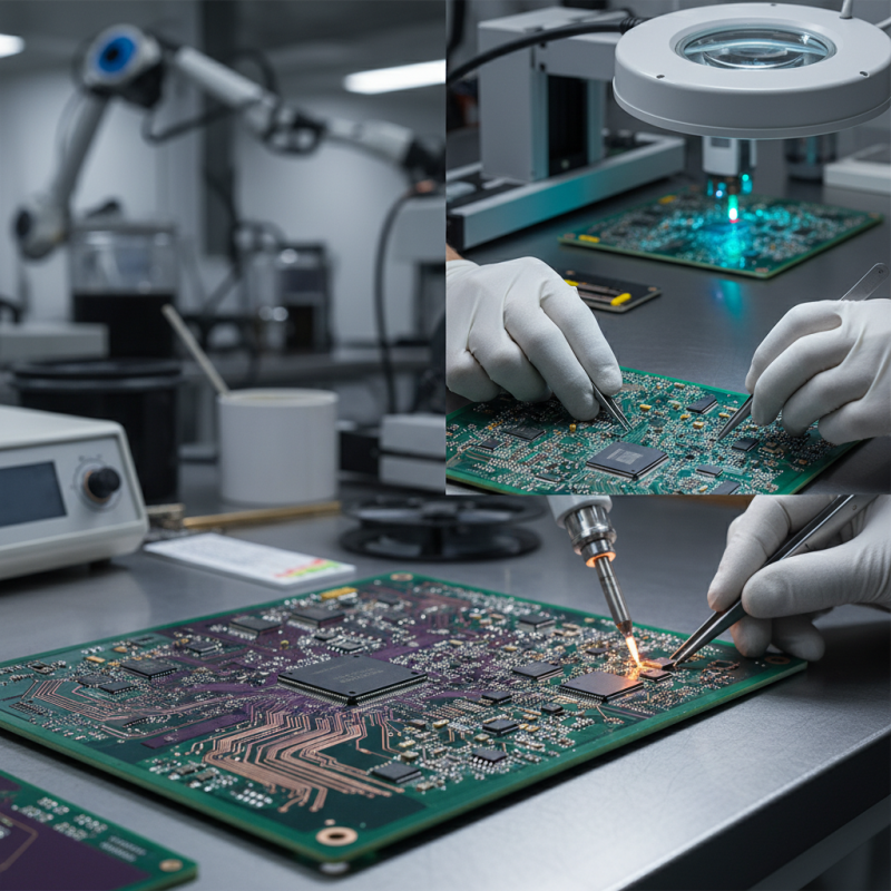
After fabrication, assembly takes place. Components are placed on the boards using techniques like soldering. Quality control is crucial at this stage. Even a tiny solder bridge can cause failures.
Tips: Inspect solder joints visually or use automated methods. Catching issues early can save a lot of headaches. Remember, a well-assembled PCB ensures better performance and reliability.
Key Steps in the PCB Fabrication Process
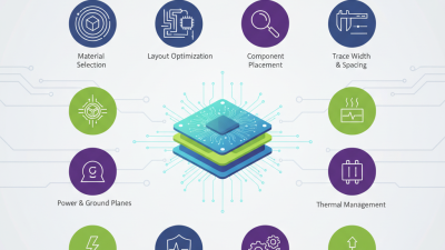
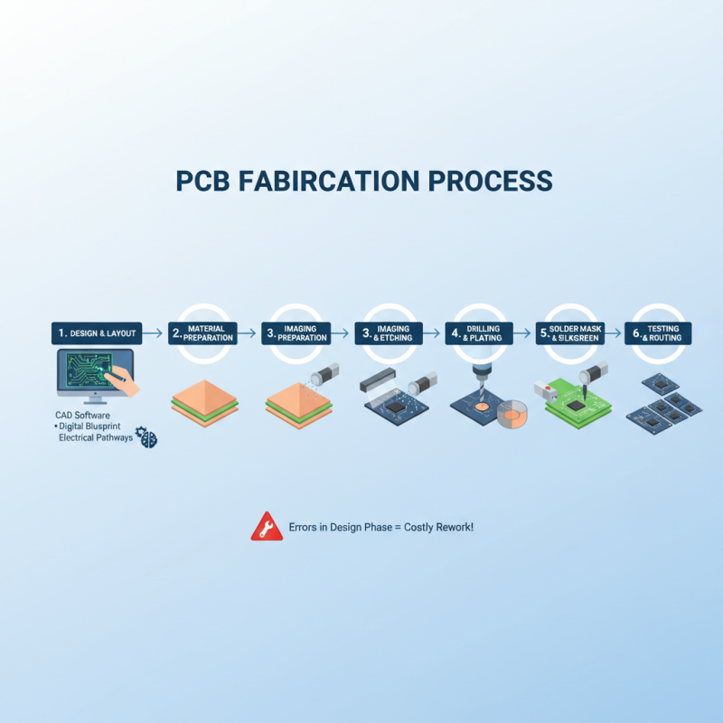
The PCB fabrication process involves several critical steps. It begins with design and layout. Designers use specialized software to create a digital blueprint of the PCB. This layout defines the electrical pathways and component placement. Mistakes in this phase can lead to costly errors later.
Once the design is finalized, the actual fabrication starts. The first physical step is to print the design onto a copper-clad board. A photo-sensitive layer helps transfer the design accurately. Next, unwanted copper is etched away, revealing the circuit pathways. These steps require precision to ensure quality.
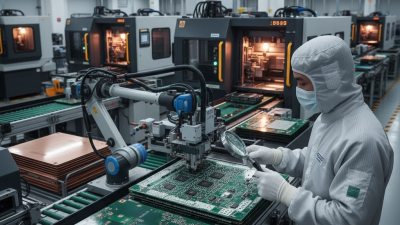
After the PCB is fabricated, assembly takes place. Components are placed onto the board using automated machines. This is where human oversight becomes essential. If components are misaligned or incorrectly placed, it can lead to malfunction. Testing is also vital after assembly. It helps identify any faults early. Addressing these issues promptly can save time and resources. The entire process reflects a balance of technology and human skill.
Techniques and Materials Used in PCB Assembly
In PCB assembly, several techniques and materials play a crucial role in ensuring performance and reliability. Surface mount technology (SMT) is widely used. This method allows components to be mounted directly on the surface of the PCB. It saves space and is efficient for mass production. However, precision is key. Misalignment during SMT can lead to failures.
Another vital technique is through-hole technology. This involves inserting components into holes drilled in the PCB. It provides better mechanical support for larger components. Yet, it can be time-consuming and may not fit all designs. The choice between SMT and through-hole often depends on the product's specific requirements.
Materials used in PCB assembly include various types of solder. Lead-free solder has become a standard due to health concerns. Still, its higher melting point presents challenges. There is also a trend towards using eco-friendly materials. While this is positive, it can affect performance. Exploring new materials and techniques is essential for future advancements. Each choice comes with trade-offs that need careful consideration.
What is PCB Fabrication and Assembly Process Explained? - Techniques and Materials Used in PCB Assembly
| Process Step |
Description |
Materials Used |
Techniques |
| Design |
Design of PCB layout using specialized software |
CAD software, schematic diagrams |
Electronic Design Automation (EDA) |
| Material Selection |
Choosing suitable substrate and conductive material |
FR-4, copper, polyimide |
Material science analysis |
| Lamination |
Bonding layers of PCB material together |
Prepregs, copper foils |
Heat and pressure techniques |
| Etching |
Removing excess copper using chemicals |
Chemical solutions (ferric chloride) |
Photolithography |
| Drilling |
Creating holes for components and vias |
Drill bits, epoxy |
CNC drilling machines |
| Plating |
Depositing metal onto the PCB surface for conductivity |
Gold, nickel, copper solutions |
Electroplating |
| Assembly |
Attaching electronic components to the PCB |
Resistors, capacitors, ICs, solder |
Soldering techniques, pick and place machines |
| Testing |
Verifying PCB functionality and quality |
Test equipment, simulation software |
Functional testing, In-circuit testing |
Quality Control Methods in PCB Manufacturing
Quality control is crucial in PCB manufacturing. It ensures that all components and processes meet specific standards. Various methods are used to maintain high quality throughout production.
One common method is visual inspection. Technicians carefully examine the boards for defects, looking for issues such as soldering errors and missing components.
Automated Optical Inspection (AOI) is another effective technique. It uses cameras to spot defects. This method increases accuracy and reduces human error. However, AOI is not foolproof. Some subtle issues can escape detection.
Regular maintenance of the inspection equipment is necessary. If not maintained, it can lead to faulty products.
Testing is vital too. Functional tests confirm that the PCB works as designed. However, these tests can be time-consuming. Some manufacturers may rush this step, compromising quality.
Implementing strict testing protocols can help. It's essential to balance speed and thoroughness. Re-evaluating current processes can lead to improvements in the overall quality of PCBs.