2026 Top Trends in PCB Manufacturing to Watch for Innovations?
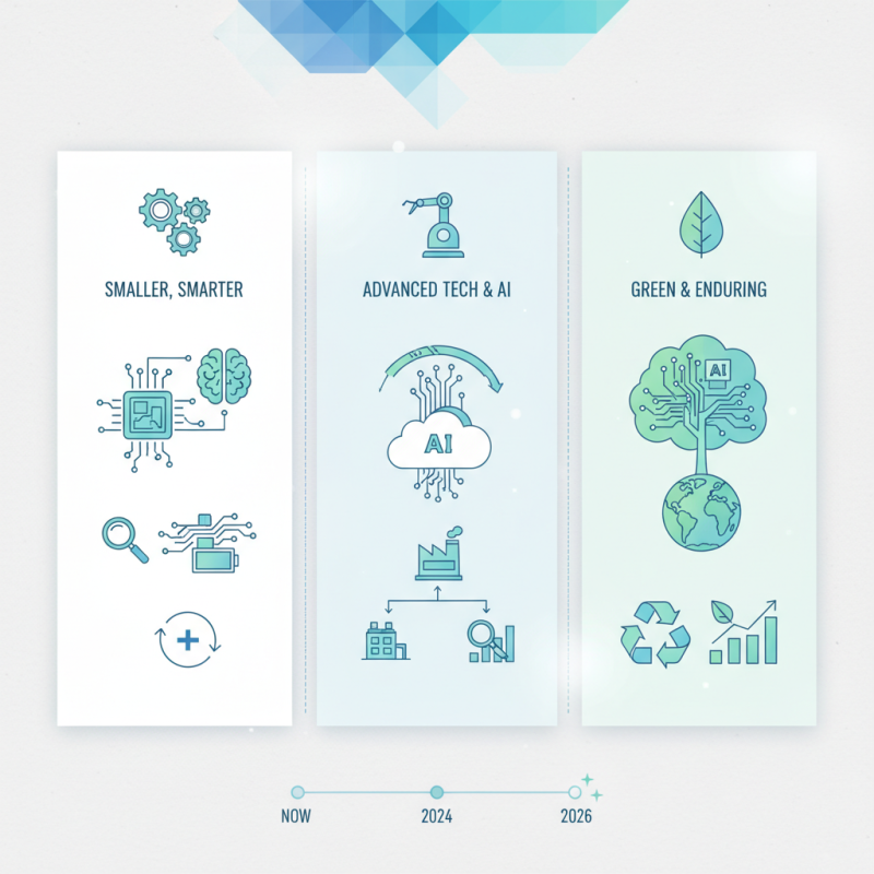
The landscape of PCB manufacturing is evolving rapidly. As we approach 2026, several trends are shaping this industry. The demand for smaller, more efficient circuits is increasing. Innovations in materials and processes are critical for meeting these needs.
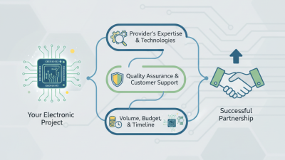
Advanced technologies are enhancing PCB capabilities. Flexible PCBs, for instance, are becoming essential for modern electronics. The integration of AI in manufacturing processes promises to streamline production and improve quality control. However, implementing these innovations poses challenges. Companies must adapt quickly to maintain competitiveness.
Sustainability is another key consideration. As environmental regulations tighten, PCB manufacturers face pressure to adopt greener practices. This transition is not straightforward and requires thoughtful strategies. Balancing innovation and sustainability will define the future of PCB manufacturing.
Emerging Technologies Reshaping PCB Manufacturing in 2026
The PCB manufacturing landscape is primed for transformation by emerging technologies in 2026. A report from a leading industry analysis firm projects that the market will grow to $84 billion. This growth will be driven by innovations such as additive manufacturing and automation. These approaches promise to reduce waste and enhance precision.
Additive manufacturing will revolutionize traditional PCB processes. Layering materials can create intricate, lightweight designs. According to recent studies, companies leveraging this technology report a 30% increase in design flexibility. However, challenges remain. Many manufacturers struggle to scale these techniques effectively. The transition is not as seamless as anticipated.
Automation is another key trend. Robotics and AI can streamline production lines. For instance, real-time monitoring can reduce defects by up to 25%. Yet, the integration of these systems may lead to workforce disruptions. Many technicians face a steep learning curve with new technologies. Striking a balance between innovation and workforce adaptation will be critical in 2026.
2026 Top Trends in PCB Manufacturing Innovations
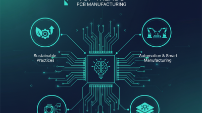
Sustainable Practices and Materials in PCB Production
Sustainable practices in PCB manufacturing are gaining momentum. The industry faces pressure to reduce environmental impact. This shift toward eco-friendly methods is becoming essential. Many manufacturers are exploring bio-based materials. These alternatives can replace traditional, harmful substances.
Recycling is another key focus. Old PCBs can be processed to recover valuable metals. This helps reduce waste and conserve resources. However, the current recycling methods are not perfect. Challenges remain in efficiency and cost-effectiveness. Innovations are necessary to overcome these hurdles.
In addition, energy-efficient production processes are being developed. These methods consume less power and generate fewer emissions. Yet, the transition to these practices requires a commitment from the industry. There is still much work to be done to achieve broad adoption. Everyone must collaborate to make the PCB sector more sustainable.
Advancements in PCB Design Software and Automation
In 2026, advancements in PCB design software are set to reshape the industry landscape. Today, software tools offer enhanced capabilities for simulating designs. Users can visualize electronic circuits in 3D before manufacturing. This reduces material waste, a critical concern for manufacturers. However, navigating the complexity of these tools can be challenging for new users. Comprehensive training is essential to fully leverage their potential.
Automation in PCB manufacturing is another trend gaining traction. Automated systems streamline repeated tasks, increasing efficiency. Tasks once done manually, like soldering and assembly, can now be performed with precision. While this boosts productivity, there are fears about job displacement. It's essential to consider how workforce training can keep pace with these changes. Balancing innovation with human talent will be crucial for future growth. Innovations must not overshadow the need for skilled workers in a shifting landscape.
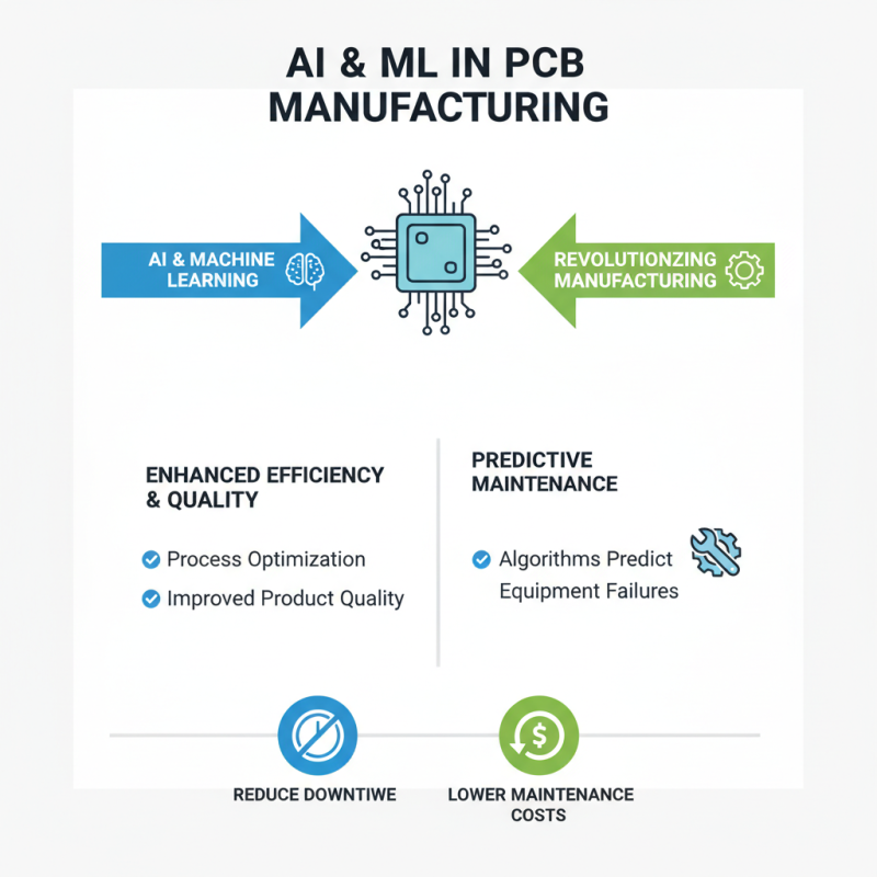
Integration of AI and Machine Learning in PCB Manufacturing Processes
The integration of AI and machine learning is revolutionizing PCB manufacturing. These technologies enhance process efficiency and product quality. For example, machine learning algorithms can predict equipment failures. This helps manufacturers reduce downtime and maintenance costs.
Furthermore, AI-driven design tools can optimize circuit layouts. These tools analyze vast data sets to suggest better configurations. They can identify potential issues early, which saves time and resources. However, reliance on these technologies raises concerns. What if the data fed into the algorithms is flawed? Inaccurate data can lead to wrong design choices.
Moreover, as organizations adopt AI, there is a learning curve. Workers need training to adapt to new systems. Transitioning too quickly can lead to errors. Companies must find a balance between automation and human oversight. This balance is crucial for sustainable innovation in PCB manufacturing.
Trends in Miniaturization and High-Density PCB Designs for Future Needs
The demand for miniaturization in PCB design is stronger than ever. As technology advances, devices become smaller yet more powerful. High-density PCB designs play a pivotal role in this evolution. Compact electronic components need to fit into tighter spaces while maintaining performance.
Innovative techniques are emerging to meet these challenges. Layer stacking and micro-via technology enable the development of smaller, denser circuits. However, this complexity can lead to issues. Manufacturing defects may increase, and testing becomes more crucial. Engineers must adapt to these higher standards and strive for improved reliability.
Importantly, as boards become miniaturized, thermal management emerges as a concern. Heat dissipation in tightly packed components can cause failures. Finding effective cooling solutions remains a challenge. Therefore, the trend towards high-density PCBs must also factor in sustainability and functionality. It's a balancing act that requires constant reflection and innovation in manufacturing processes.