Understanding PCB Circuit Boards: The Backbone of Modern Electronics Explained
In the ever-evolving landscape of modern electronics, the significance of the PCB circuit board cannot be overstated. As the backbone of electronic devices, PCB circuit boards facilitate complex interconnections, enabling seamless functionality across various applications. According to a 2022 market research report by MarketsandMarkets, the global PCB market is projected to reach
USD 88.78 billion by 2025, growing at a compound annual growth rate (CAGR) of 4.5%. This growth is driven by advancements in technology and the increasing demand for consumer electronics, automotive applications, and communication devices. Understanding the intricacies of PCB circuit boards is essential for engineers and designers who aspire to innovate within this dynamic sector. This guide will delve into the fundamental aspects of PCB circuit boards, exploring their design, manufacturing processes, and their pivotal role in shaping the future of electronics.
The Evolution of PCB Technology in Modern Electronics
The evolution of PCB technology in modern electronics has been marked by significant advancements that have transformed how electronic devices are designed and manufactured. Initially, PCBs were rudimentary, often comprising a simple, flat board with hand-drawn circuits. As demand for more compact and efficient electronic systems grew, the industry shifted towards automated manufacturing processes and complex multilayer designs. This transition allowed for denser circuit layouts, enabling manufacturers to increase functionality without enlarging the physical footprint of devices.
In recent years, innovations such as flexible PCBs and HDI (High-Density Interconnect) boards have emerged, offering even greater design possibilities. Flexible PCBs facilitate a new level of versatility by allowing devices to be lightweight and adaptable in structure, which is especially important in wearable technologies and portable gadgets. Furthermore, advancements in materials, such as improved dielectric substrates and solder mask technologies, have enhanced thermal performance and reliability. As we continue to push the boundaries of what is possible in electronics, the evolution of PCB technology remains critical in shaping the capabilities and performance of modern devices.
Understanding PCB Technology Evolution
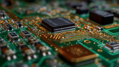
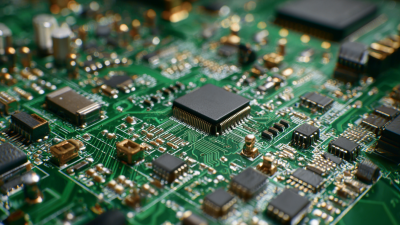
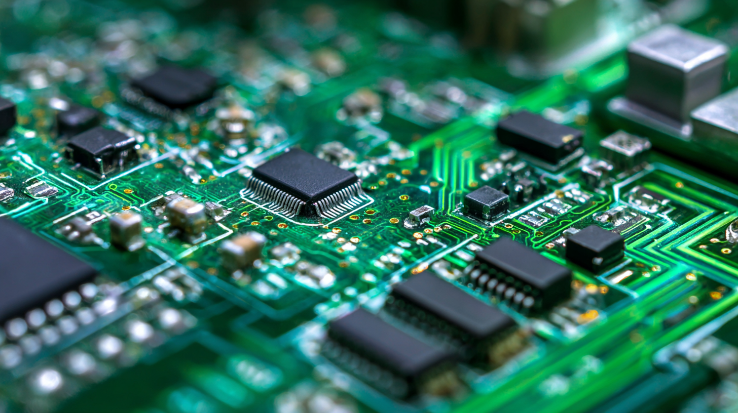
Key Components and Materials Used in PCB Manufacturing
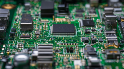
 Printed Circuit Boards (PCBs) are essential components in modern electronics, serving as the backbone for connecting various electronic elements.
Understanding the key components and materials used in PCB manufacturing is crucial for appreciating their role in the technological landscape. One of the primary materials used is copper, which provides conductivity and is often paired with substrates like FR-4 for insulation and support.
The global market for copper foil, a critical input for PCBs, is expected to see significant growth, reflecting the increasing demand for efficient conductors in electronic devices.
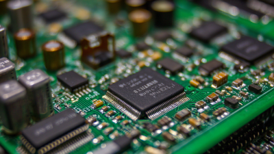
Printed Circuit Boards (PCBs) are essential components in modern electronics, serving as the backbone for connecting various electronic elements.
Understanding the key components and materials used in PCB manufacturing is crucial for appreciating their role in the technological landscape. One of the primary materials used is copper, which provides conductivity and is often paired with substrates like FR-4 for insulation and support.
The global market for copper foil, a critical input for PCBs, is expected to see significant growth, reflecting the increasing demand for efficient conductors in electronic devices.
When exploring PCB manufacturing, it is essential to consider the latest advancements in materials. Innovations in copper-based materials have positioned companies in this segment for rapid growth as the electronic information industry transitions.
Furthermore, leveraging twin-drives of technology and performance is pivotal for companies seeking to establish benchmarks in the PCB sector. For instance, utilizing optical PCBs in advanced applications showcases how these materials are evolving to meet complex industry needs.
Tips:
- Always keep abreast of the latest materials being used in PCB manufacturing as they can impact performance and durability.
- Consider sustainable practices in PCB design and manufacturing to align with growing environmental concerns.
- Stay informed about market trends, as they can influence sourcing strategies and investment opportunities in the PCB industry.
Market Trends: Growth and Demand for PCBs in Various Industries
The demand for printed circuit boards (PCBs) is witnessing significant growth across various industries, driven by the increasing adoption of advanced technologies. According to a report by Market Research Future, the global PCB market is expected to reach approximately $85 billion by 2025, growing at a compound annual growth rate (CAGR) of about 4.5%. This surge is particularly pronounced in sectors such as consumer electronics, automotive, and medical devices, where the integration of sophisticated electronic components is pivotal.
One of the key trends shaping the PCB market is the rise of electric vehicles (EVs). As manufacturers push towards sustainability, the need for high-performance PCBs that support complex circuitry and efficient power management systems is becoming essential. A report from Fortune Business Insights indicates that the automotive PCB segment could reach over $20 billion by 2025, highlighting the impact of technological advancements on market dynamics. Furthermore, the healthcare sector is increasingly utilizing PCBs in the development of advanced diagnostic and monitoring devices, contributing to the overall demand for innovative PCB solutions.
Challenges and Innovations in PCB Design and Fabrication
The printed circuit board (PCB) industry is currently navigating a landscape marked by rapid technological advancements and increasing complexity. According to a report by market research firm ResearchAndMarkets, the global PCB market is expected to reach approximately $83 billion by 2025, growing at a compound annual growth rate (CAGR) of around 4.5%. This growth is largely driven by the demand for miniaturized devices with high functionality, which poses unique challenges in design and fabrication. Innovators in the field are focusing on advanced materials, multilayer designs, and automated manufacturing processes to stay competitive.
One significant challenge in PCB design is managing thermal dissipation while maintaining efficient performance. As electronics grow smaller and more powerful, the risk of overheating increases. Designers are adopting thermal simulation tools to predict and mitigate heat build-up within PCBs. It is essential for engineers to prioritize heat management in their designs, not only for operational efficiency but also to extend the lifespan of their devices.
**Tip:** When designing PCBs, consider integrating heat sinks or thermal vias to improve heat dissipation. Furthermore, staying updated with the latest CAD software can streamline the design process and aid in addressing potential fabrication issues early on. Reliable suppliers and rigorous testing protocols can significantly enhance the quality and reliability of finished boards.
The Future of PCB Technology: Trends and Predictions for 2025 and Beyond
As we look toward 2025 and beyond, the landscape of PCB technology is set for transformative changes driven by advancements in materials, manufacturing processes, and design methodologies. One key trend is the increasing integration of flexible and printed circuit boards, allowing for lightweight and compact electronics that can conform to various shapes. This flexibility is essential for the rise of wearable devices and Internet of Things (IoT) applications, where space savings and design versatility are paramount.
Another significant trend is the growing demand for high-speed and high-frequency PCBs. As data transmission speeds continue to increase, traditional PCB designs will need to evolve to handle greater bandwidths while minimizing signal loss. Innovations in substrate materials and layer stacking techniques will play a crucial role in achieving these performance improvements. Additionally, sustainability will shape the future of PCB manufacturing, with more companies focusing on eco-friendly materials and processes to reduce waste and energy consumption. These trends not only signify a pivotal shift in PCB technology but also highlight the ongoing need for innovation to meet the ever-evolving demands of modern electronics.
Understanding PCB Circuit Boards: The Backbone of Modern Electronics Explained
| Aspect |
Details |
| Material Types |
FR-4, Polyimide, Rogers |
| Layer Count |
Single-sided, Double-sided, Multi-layer (up to 64) |
| Applications |
Consumer Electronics, Automotive, Industrial Control |
| Manufacturing Technologies |
Surface Mount Technology (SMT), Through-Hole Technology |
| Future Trends |
Flexible PCBs, HDI PCBs, Integration with IoT |
| Sustainability |
Green PCB technologies, Biodegradable materials |
| Key Challenges |
Supply chain issues, Component shortages, Manufacturing costs |