Understanding the Journey of PCB Fabrication and Assembly from Concept to Creation
The journey of PCB fabrication and assembly, from initial concept to final creation, is a critical process in the electronics manufacturing industry. According to a recent report by IPC, the global PCB market was valued at approximately $65 billion in 2021, with an expected growth rate of 3.5% annually through 2027. This growth is fueled by the increasing demand for advanced electronic devices across various sectors including consumer electronics, automotive, and telecommunications. The complexity of PCB designs has evolved dramatically, requiring manufacturers to adopt cutting-edge technologies and efficient workflows to meet stringent quality standards. As we explore the intricate stages of PCB fabrication and assembly, it becomes clear that understanding this journey is essential for optimizing production efficiency and ensuring the reliability and performance of electronic products in a rapidly advancing technological landscape.
The Transition from Idea to Reality: An Overview of PCB Fabrication
The transition from the initial concept to the realization of printed circuit boards (PCBs) involves an intricate process of fabrication and assembly. In today's rapidly evolving technological landscape, the principles of Industry 4.0 play a crucial role in optimizing these processes, enabling businesses to enhance efficiency and sustainability. The integration of digital technologies allows manufacturers to make data-driven decisions, thus minimizing waste and aligning with the circular economy ideals. By embracing these innovative practices, companies can significantly reduce their environmental footprint while meeting the growing demand for electronic components.
**Tips:** To streamline your PCB design process, consider using advanced simulation tools that can predict potential issues before physical fabrication. This proactive approach can save time and resources, ensuring a smoother transition from design to assembly. Additionally, implementing automated inspection systems during the assembly phase can help maintain high-quality standards, further reducing waste and improving overall efficiency.
Embracing imagination as a key driver for innovation is essential in this journey. As challenges like climate change loom, the PCB industry has the unique opportunity to lead the way in adopting eco-friendly materials and methods. By fostering a culture of creativity and adaptability, PCB manufacturers can not only innovate but also contribute positively to a sustainable future.
Understanding the Journey of PCB Fabrication and Assembly from Concept to Creation
| Phase |
Description |
Duration (Days) |
Key Activities |
| Concept Design |
Initial design and requirements gathering for PCB |
10 |
Brainstorming, sketching, and schematic creation |
| Layout Design |
Creating the physical layout of the PCB |
15 |
PCB layout drafting using CAD tools |
| Prototyping |
Fabrication of the initial prototype for testing |
20 |
Ordering materials and manufacturing the prototype |
| Assembly |
Assembling all components onto the PCB |
12 |
Soldering and placement of electronic components |
| Testing |
Verifying the functionality and reliability of the PCB |
8 |
Functional tests, debugging, and validation |
| Mass Production |
Scaling up production for market readiness |
30 |
Production planning, inventory management, and logistics |
Key Phases in PCB Design and Prototyping for Successful Assembly
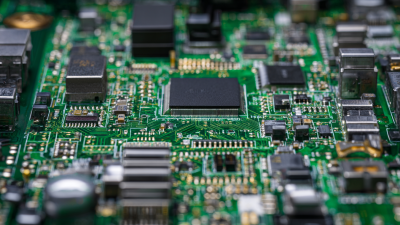
The journey of PCB fabrication and assembly is complex, involving several critical phases to ensure successful design and prototyping. One of the pivotal stages in this process is the design phase, where engineers utilize tools such as Computer-Aided Design (CAD) software. According to a report by IPC, over 60% of PCB design errors stem from inadequate planning and design reviews. This highlights the necessity of thorough verification and iterative designs to minimize costly modifications later in the production process.
Once the design is finalized, the prototyping phase begins, which allows engineers to create a physical representation of the PCB. Rapid prototyping techniques, such as 3D printing and CNC machining, have drastically reduced lead times, enabling manufacturers to produce functional prototypes in as little as 48 hours. The 2022 Global PCB Market Report indicates that nearly 75% of companies now rely on prototypes to identify design flaws early, ensuring that the final assembly meets performance expectations. This highlights that investing time in the prototyping phase ultimately leads to higher-quality products and more efficient manufacturing processes.
Exploring Materials and Technologies in Modern PCB Manufacturing
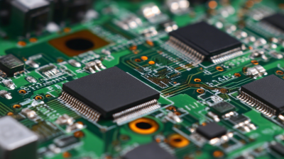
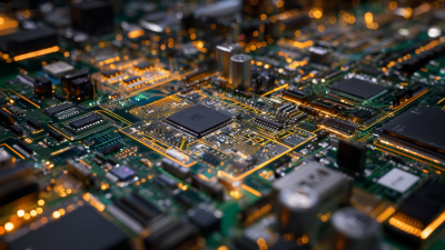
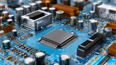
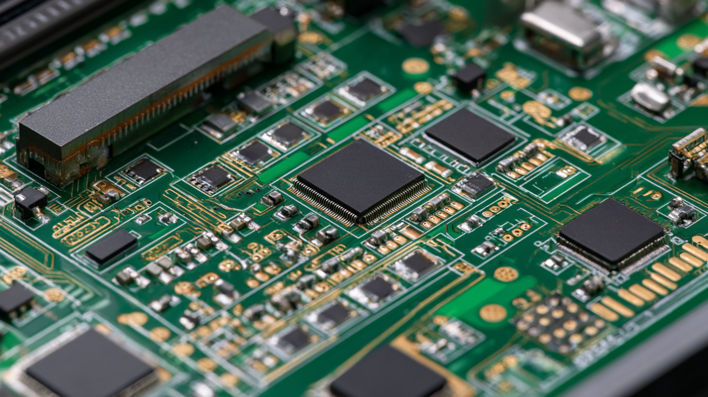
The journey of PCB fabrication and assembly begins with a meticulous selection of materials, as the right substrates and conductors are crucial for optimal performance. Modern PCBs often utilize a variety of materials, including FR-4, a flame-retardant fiberglass, and polyimide for flexible circuits. These materials provide the necessary electrical insulation and mechanical stability required to withstand heat and environmental stresses. Alongside traditional copper traces, innovations such as conductive inks and silver nanowires are gaining traction, allowing for enhanced flexibility and new design possibilities.
Advancements in manufacturing technologies have also transformed PCB production. Techniques such as automated optical inspection (AOI) and selective soldering improve precision and efficiency, reducing error rates in assembly. Moreover, methods like 3D printing are beginning to emerge, enabling rapid prototyping and customization, which are essential in a fast-paced market. The integration of IoT and smart manufacturing technologies into the PCB production process allows real-time monitoring and data analytics, enhancing production quality and traceability. These developments are paving the way for more sophisticated electronic devices, emphasizing the importance of understanding both materials and technologies in modern PCB manufacturing.
Quality Control and Testing Practices in PCB Fabrication and Assembly
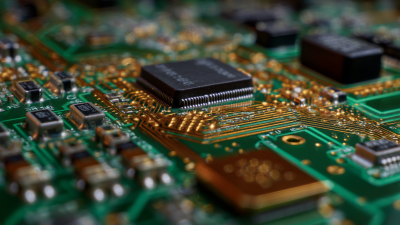
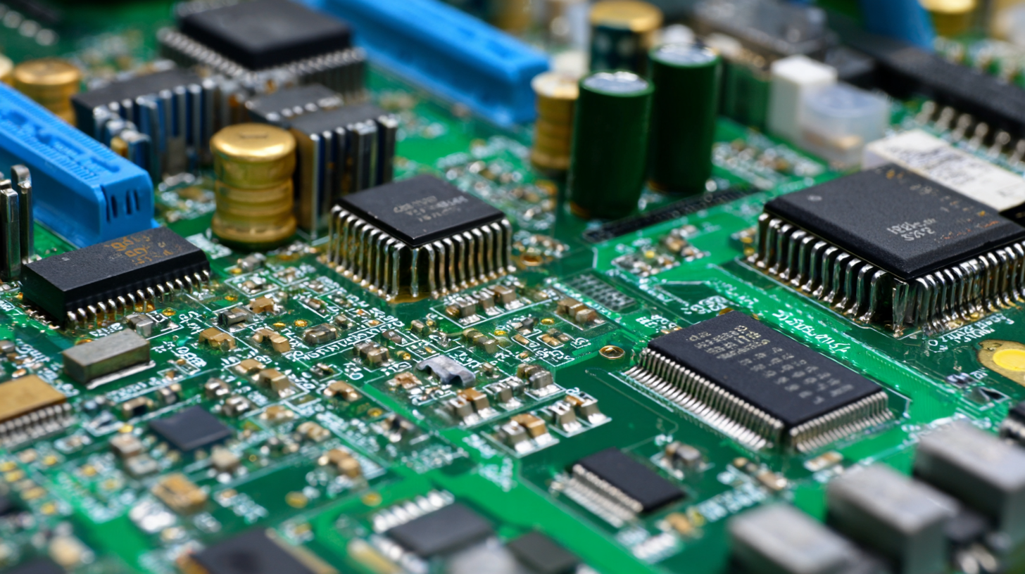
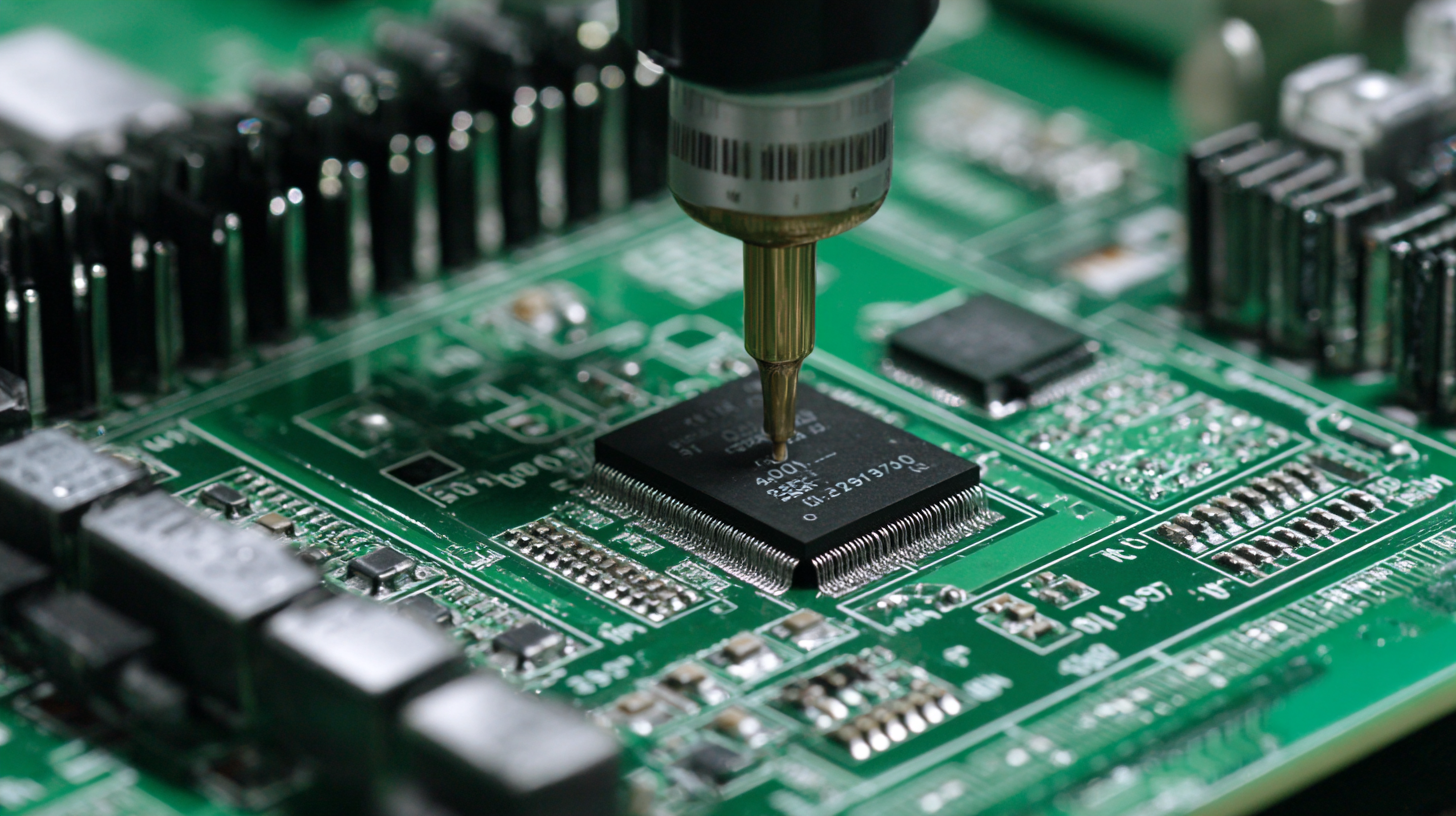
Quality control and testing practices are critical components in the PCB fabrication and assembly process. From the early stages of design to the final assembly, ensuring high standards is essential for reliability and performance. One of the key techniques employed is in-process inspections, where each stage of production undergoes rigorous checks. Visual inspections, automated optical inspections (AOI), and X-ray inspections are commonly used to detect defects before proceeding to the next phase, thus minimizing errors and enhancing quality.
In addition to in-process inspections, thorough testing post-assembly is crucial. Functional testing assesses the performance of the assembled PCB to ensure it meets design specifications. Electrical tests, including continuity tests and impedance measurements, help identify any potential issues that could lead to failures in the final product. Moreover, environmental testing simulates real-world conditions to evaluate the PCB's durability and reliability. By implementing these quality control measures and testing practices, manufacturers can ensure that each PCB that leaves their facility is capable of performing optimally in its intended application, thereby safeguarding customer satisfaction and trust.
Streamlining Supply Chain Management for Efficient PCB Production
In today's rapidly evolving electronics manufacturing sector, streamlining supply chain management (SCM) is crucial for enhancing PCB production efficiency. Recent advancements highlight how technologies like artificial intelligence and robotic automation are playing significant roles in optimizing supply chains. For instance, a report indicates that the implementation of AI can reduce lead times and improve inventory accuracy, with organizations witnessing a potential decrease in operational costs by up to 20% through advanced forecasting and resource management techniques.
Additionally, the integration of Enterprise Resource Planning (ERP) systems with SCM technologies has become fundamental to driving operational efficiencies. As revealed by industry analyses, manufacturers utilizing ERP solutions can achieve up to a 30% increase in productivity. This synergy not only minimizes silos within organizations but also promotes real-time collaboration across various stages of PCB fabrication and assembly, leading to quicker time-to-market for innovative electronics. Companies leveraging these technologies are better positioned to respond to shifts in consumer demands, ensuring a competitive edge in an increasingly complex global landscape.