Essential Tips for Effective Circuit Board Design for Buyers?
In the realm of circuit board design, expertise is crucial for creating efficient and reliable products. Renowned expert Dr. Jane Smith, a leader in electronics engineering, once said, "Good design shapes innovation." This insight underscores the significance of strategic planning in circuit board design.
Designing circuit boards requires a meticulous approach. Each component, trace, and layer plays a vital role in overall functionality. Think about power distribution, signal integrity, and thermal management. These elements need careful consideration. Often, designers overlook the importance of layout optimization. Poor layout can lead to issues like electromagnetic interference and signal degradation, which can compromise performance.
Moreover, effective communication within a design team is essential. Misunderstandings can lead to costly mistakes. Each team member must understand their role in the circuit board design process. Continuous learning and adaptation are necessary. Even seasoned professionals face challenges. The industry evolves rapidly, and staying updated is key. Embracing these insights can enhance circuit board design, leading to better products and innovation.

Fundamentals of Circuit Board Design for Buyers
When diving into the fundamentals of circuit board design, understanding the key aspects can significantly enhance the effectiveness of your project. A well-designed circuit board can reduce manufacturing costs by up to 30%, according to industry reports. Buyers should focus on aspects like board layout, material selection, and thermal management for optimal performance.
Consider these crucial tips: ensure adequate spacing between components to prevent overheating. Use multi-layer boards for complex designs as they can reduce electromagnetic interference. Additionally, utilizing simulation software early in the design process allows for identifying potential issues before fabrication, saving time and resources.
Buyers must keep in mind that while design software offers powerful tools, they are not foolproof. Miscommunication between engineers can lead to flawed designs. A report from Design News highlights that nearly 40% of design teams experience setbacks due to misunderstandings. Regular check-ins and design reviews are essential. Testing prototypes thoroughly can also expose flaws that simulations might miss. Reliable circuit board design balances creativity with structured analysis for the best results.
Essential Tips for Effective Circuit Board Design for Buyers
| Design Aspect |
Tip |
Importance |
| Component Placement |
Place components logically to minimize trace lengths. |
Reduces noise and improves performance. |
| Trace Width |
Calculate trace width based on current carrying capacity. |
Prevents overheating and ensures reliability. |
| Ground Planes |
Utilize ground planes to enhance EMI performance. |
Improves signal integrity and reduces interference. |
| Layer Stackup |
Design optimal layer stack for impedance control. |
Essential for high-frequency applications. |
| DRC Rules |
Follow Design Rule Check (DRC) guidelines thoroughly. |
Prevents manufacturing errors and enhances yield. |
Key Considerations When Selecting PCB Materials
When selecting PCB materials, understanding the thermal management capabilities is crucial. According to industry reports, nearly 30% of PCB failures stem from inadequate heat dissipation. High-quality materials like FR-4 provide good thermal stability, but emerging options, such as aluminum and ceramic substrates, enhance performance. These materials are more efficient for high-frequency applications. However, many buyers overlook them, leading to suboptimal designs.
Mechanical properties also play a vital role in PCB performance. A study shows that over 40% of mechanical failures occur due to the wrong material choice. Rigid materials may be suitable for conventional applications, while flexible materials are essential for wearable devices. Not considering these factors can result in significant production delays and increased costs. Buyers should consult with specialists to navigate these complexities.
Cost is another crucial factor in material selection. The average cost of PCB materials has seen fluctuations, with some high-performance options reaching up to 25% more than traditional alternatives. This adds pressure to engineers who need to balance performance and budget. Understanding the trade-offs in material selection can lead to more effective and reliable circuit board designs.
Understanding Circuit Board Layout Techniques
When designing a circuit board, layout techniques play a crucial role. A well-thought-out layout minimizes interference and enhances performance. Start with a clear schematic. It’s essential to understand how each component interacts. Use this as your blueprint.
Pay attention to component placement. Elements that communicate should be close together. This reduces the length of traces, which helps control resistance and capacitance. Keep high-frequency components separated from others. This can prevent signal degradation. Ground planes are vital. They provide a solid reference point and help reduce electromagnetic interference.
Testing and revisions are often overlooked. After initial design, a prototype is critical. Errors often surface in real-world applications. Analyze performance carefully. Every tweak can lead to significant improvements. Never underestimate the importance of iterative feedback in circuit board design. Your layout process should evolve with these insights.
Importance of Component Placement and Routing
Component placement and routing are vital in circuit board design. Proper placement impacts the functionality and performance of the board. Components should be organized logically. This reduces the complexity during assembly and troubleshooting. Arranging components close to related parts minimizes trace lengths. Shorter traces help to decrease inductance and capacitance effects, enhancing signal integrity.
The routing of traces is equally important. Traces should follow a clear path. Avoid sharp angles, as they can create impedance issues. Strive for a balanced distribution of power and ground planes to prevent potential noise problems. When components are densely packed, careful routing becomes a challenge. It demands creativity and patience. Sometimes, the ideal layout is not achievable on the first try. Designers must adapt and refine their approaches.
Regular reviews of initial designs can uncover potential improvements. Seeking feedback from others can provide new perspectives. Reflecting on your design choices fosters growth in skills. Mistakes in placement and routing can be costly. They can lead to performance failures or increased costs. Embracing a mindset of continual learning and improvement is essential for success in designing effective circuit boards.
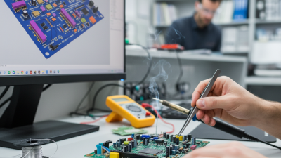
Testing and Validation Methods for Circuit Boards
When designing circuit boards, testing and validation are critical steps. These processes ensure that your designs function as intended. Effective testing involves both functional and performance checks. Using automated testing tools can significantly streamline this process. However, manual inspection should not be overlooked. Observing solder joints and component placements can reveal issues early on.
Incorporating a robust validation plan is necessary. This plan should include stress tests to evaluate how the board reacts under various conditions. Heat, humidity, and voltage fluctuations can impact performance. If these factors are not considered, the board may fail in real-world applications.
Documentation is key in this phase. Recording test results not only helps in troubleshooting but also in future design iterations. Reflecting on past tests can provide valuable insights. Sometimes, the unexpected failures offer the most learning opportunities. Regularly revising testing methods can lead to improved outcomes. It is important to remember that no design is perfect from the start. Continuous improvement is essential in circuit board design.