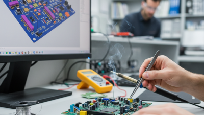
Printed circuit board design is the quiet engineering work behind reliable electronic products. It determines how signals travel, how heat escapes, and how safely components operate. A board may look like a flat green surface, but its copper layers form a carefully controlled electrical system.
Experienced designers consider impedance, return paths, power distribution, grounding, thermal relief, and component placement before routing begins. They also review manufacturing limits, inspection access, assembly tolerances, and long-term service needs. Henry W. Ott, a respected electromagnetic compatibility engineer, stated, “The most important thing in controlling EMI is to control the current paths.” That principle remains practical. A poorly planned return path can create noise, unstable communication, or unexpected emissions.
Small details matter. A misplaced decoupling capacitor can weaken power integrity. A narrow trace near a hot regulator may suffer unnecessary stress. Sharp corners, crowded vias, and incomplete design rules can also cause production problems. Yet no layout is perfect. Engineers must balance performance, cost, size, schedule, and manufacturability.
That balance explains why printed circuit board design is important. It connects theoretical calculations with physical experience on the workbench and the factory floor. A simulation may predict success, but prototypes can reveal connector noise, uneven heating, or difficult assembly. Careful testing is essential. So is honest review.
Good design is more than making connections. It creates a dependable product that can be manufactured, tested, repaired, and improved. This article examines the main reasons printed circuit board design influences product quality, reliability, safety, and commercial success.
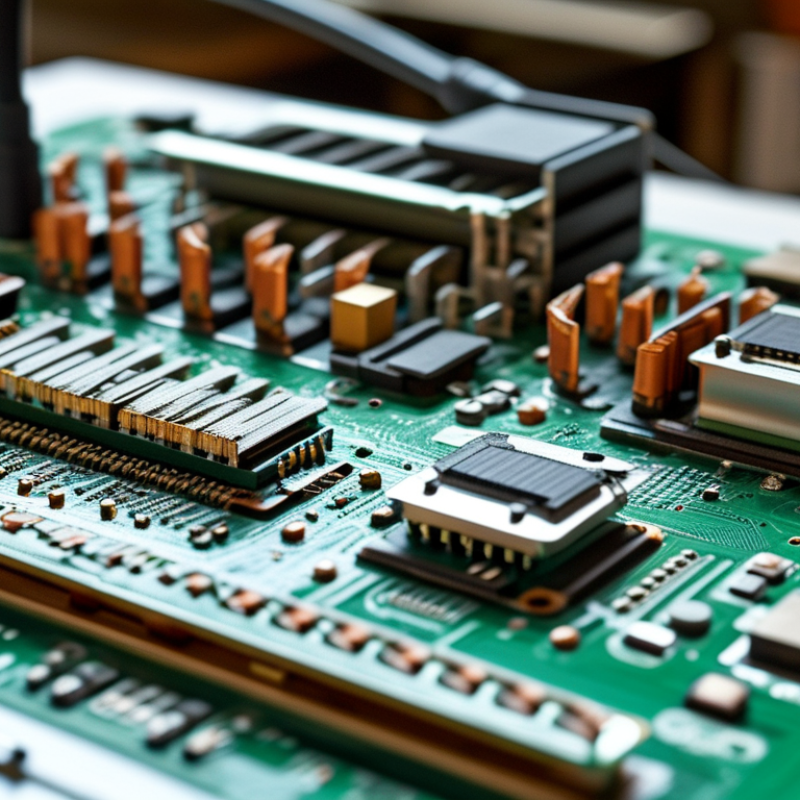
Printed circuit board design is important because it turns a circuit idea into a manufacturable, testable assembly. What does that work involve? It combines schematic planning, component placement, routing, layer selection, and design verification. Each decision affects signal quality, heat, mechanical strength, and production cost. A compact board is not automatically a good board.
In practical design reviews, engineers first confirm the circuit requirements and operating environment. They then place critical components near related parts to shorten connections. High-speed signals need controlled paths and careful spacing. Power routes usually require wider copper traces. Grounding must provide a stable return path. Thermal areas may need copper planes, vias, or improved airflow. Small details matter. A misplaced connector can make assembly and servicing difficult.
Designers also check clearances, hole sizes, trace widths, and manufacturing limits before releasing files. Simulation can reveal voltage drops, heat buildup, or signal interference. Prototype testing adds evidence that software checks cannot provide. A first layout is rarely perfect. I have seen reasonable designs fail because a test point was forgotten or a screw blocked a component. That kind of mistake is frustrating, but it improves the next revision. Good documentation, peer review, and version control make changes easier to track and verify.
| Design dimension | What the design work involves | Why it is important | Typical measurable output | Risk when overlooked |
|---|---|---|---|---|
| Electrical schematic | Defines component connections, power rails, signal paths, protection circuits, and test points before physical layout begins. | Creates the electrical blueprint and helps identify incorrect connections before fabrication. | Complete netlist, design-rule checks, power-rail documentation, and approved bill of materials. | Open circuits, short circuits, missing functions, or expensive board revisions. |
| Layer stack-up | Selects the number of copper layers, dielectric materials, reference planes, and board thickness. | Controls signal return paths, electromagnetic behavior, manufacturability, and power distribution. | Documented layer count, finished thickness, copper weights, dielectric thicknesses, and impedance targets. | Excessive noise, poor signal integrity, warpage, or incompatibility with fabrication requirements. |
| Component placement | Positions components according to signal flow, thermal behavior, mechanical constraints, and assembly access. | Shortens critical connections, improves cooling, and supports reliable automated or manual assembly. | Placement clearance checks, keep-out compliance, connector alignment, and thermal-distribution review. | Longer traces, hot spots, assembly defects, inaccessible test points, or mechanical interference. |
| Routing and signal integrity | Routes traces while managing trace width, spacing, return paths, differential pairs, vias, and controlled-impedance lines. | Maintains signal quality and timing, particularly for fast digital, clock, radio-frequency, and differential signals. | Completed connectivity, length-matching records where required, impedance calculations, and clearance results. | Reflections, crosstalk, timing errors, intermittent operation, or electromagnetic interference. |
| Power distribution | Designs power and ground planes, decoupling capacitors, current paths, voltage conversion, and protection features. | Provides stable supply voltage and reduces voltage drop and supply noise during changing loads. | Voltage-drop analysis, current-density review, capacitor placement records, and documented rail limits. | Brownouts, resets, overheating, excessive ripple, or premature component failure. |
| Thermal management | Uses copper areas, thermal vias, heat sinks, airflow paths, and component spacing to manage heat. | Keeps components within their rated operating temperatures and improves long-term reliability. | Estimated junction temperature, thermal-resistance analysis, copper-area review, and temperature-test results. | Thermal shutdown, accelerated aging, solder-joint fatigue, or reduced service life. |
| Manufacturability | Applies suitable trace widths, spacing, drill sizes, annular rings, solder-mask clearances, and panelization rules. | Makes the board practical to fabricate and reduces defects, scrap, and production delays. | Design-for-manufacturing report, fabrication drawing, drill file, layer artwork, and panel plan. | Unfabricated features, low production yield, solder bridges, or additional manufacturing cost. |
| Assembly and testability | Defines component orientation, fiducials, polarity markings, inspection access, test pads, and programming interfaces. | Supports accurate assembly, efficient inspection, debugging, repair, and production testing. | Assembly drawings, pick-and-place data, test-point list, polarity checks, and inspection coverage. | Incorrect component orientation, difficult troubleshooting, missed defects, or higher labor requirements. |
| Electromagnetic compatibility | Controls current-loop areas, high-speed transitions, shielding, filtering, grounding, and separation of noisy and sensitive circuits. | Reduces unwanted emissions and susceptibility to interference from internal or external sources. | Grounding plan, filter placement review, return-path analysis, and pre-compliance test results. | Failed compliance testing, communication errors, unstable sensors, or interference with nearby equipment. |
| Mechanical integration | Coordinates board outline, mounting holes, connector locations, enclosure clearances, fasteners, and component height limits. | Ensures the finished board fits correctly and withstands installation and operating conditions. | Validated board outline, 3D clearance review, mounting-hole positions, and connector alignment. | Enclosure conflicts, damaged connectors, mounting stress, or inability to install the assembly. |
| Reliability and compliance | Reviews material selection, spacing, environmental conditions, safety requirements, inspection criteria, and revision control. | Improves product durability, traceability, safety, and conformity with applicable technical requirements. | Controlled design files, verification records, environmental limits, inspection criteria, and release documentation. | Field failures, safety concerns, inconsistent revisions, or delays during qualification. |