Electronic Contract Manufacturing Service Provider in California

How to Choose the Best Circuit Board Design?

Choosing the best circuit board design is not simply a matter of adding more layers or selecting premium materials. It is a practical decision shaped by electrical performance, manufacturing limits, operating conditions, and total cost. A board that works perfectly in a laboratory may fail inside a hot enclosure with vibration, dust, and restricted airflow.

Eric Bogatin, a respected signal-integrity engineer and educator, states, “Signal integrity is not a black art.” His message is valuable because reliable circuit board design depends on measurable factors. Stack-up planning, controlled impedance, return paths, trace spacing, grounding, and component placement all deserve careful attention. For example, a high-speed USB pair routed beside a noisy switching node can create unexpected emissions. A poorly placed thermal via may also leave a regulator dangerously hot.

This guide compares practical design choices for different applications. It considers prototype speed, production volume, layer count, material selection, testing, and long-term reliability. IPC guidance and the fabricator’s design-for-manufacturing rules should support every major decision. Experienced engineers also review the design with assembly and testing teams before release.

Still, no selection method is flawless. A cheaper two-layer board may be suitable for a sensor, but unsuitable for dense digital circuitry. I have seen designs look elegant on screen and become difficult to assemble in production. That gap matters. The best circuit board design is the one that meets electrical needs, survives its real environment, and remains manufacturable at the expected scale.
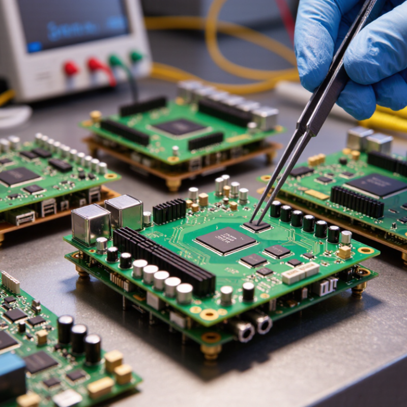
How to Choose the Best Circuit Board Design?

Define the Circuit Board’s Purpose and Performance Requirements

How to Choose the Best Circuit Board Design?

Define the Circuit Board’s Purpose and Performance Requirements

A reliable circuit board begins with a clear job description. Will it control a motor, collect sensor data, or process wireless signals? Each purpose creates different electrical and physical demands. Write the operating voltage, current range, signal speed, and expected service life before selecting a layout approach.

Define the environment too. A board inside a factory machine may face dust, vibration, heat, and electrical noise. A portable device may need low power and resistance to repeated flexing. Record temperature limits, enclosure size, connector locations, and maintenance access. These details prevent attractive designs from failing during real operation.

Performance requirements should be measurable. For example, specify a maximum signal error, start-up time, standby current, or allowable temperature rise. Engineers can then verify the design through simulation, prototype testing, and documented inspections. Thermal imaging may reveal a hot regulator, while an oscilloscope can expose unstable edges or unwanted noise.

Requirements often change.

That is normal, but undocumented changes create confusion. A first draft may overlook cable movement or heat from nearby components. Review the assumptions with manufacturing, testing, and field-service teams. Build in reasonable margins, not unlimited ones, because extra capacity can increase cost and board size. A design that meets today’s figures may still need revision after testing. That is not failure; it is useful evidence.

Compare PCB Types, Materials, and Layer Configurations

How to Choose the Best Circuit Board Design?

Compare PCB Types, Materials, and Layer Configurations

Choosing the right circuit board begins with matching physical demands to PCB construction. A rigid board suits stable enclosures and straightforward assembly. Flexible circuits bend around hinges, displays, or narrow mechanical spaces. Rigid-flex designs reduce connectors and improve reliability in moving products. They cost more. For common prototypes, FR-4 offers a practical balance of price, strength, and electrical performance. Its glass-reinforced epoxy handles moderate heat and supports many layer configurations. High-frequency designs may need low-loss laminates to protect signal quality. Metal-core boards move heat away from powerful LEDs or converters. Material choice affects drilling, soldering, impedance, and long-term stability.

Layer count should follow routing density and signal behavior, not habit. A two-layer PCB keeps fabrication simple and works well for basic controls. Four-layer stackups provide dedicated power and ground planes, often improving noise control. More layers add cost and inspection challenges. They can also reduce routing congestion. I once selected a two-layer layout to control budget. That assumption was wrong. The final wiring became crowded, and manual rework increased. Copper thickness, dielectric spacing, and via size deserved earlier review. Check thermal paths near high-current components. Keep sensitive traces away from switching nodes. Blind and buried vias can save space, yet they complicate fabrication and testing. Ask the manufacturer about realistic tolerances before locking the stackup. Small changes in layer spacing can affect impedance enough to require another prototype.

Evaluate Component Placement, Routing, and Signal Integrity

How to Choose the Best Circuit Board Design?

Component placement should begin with current paths and return paths, not the schematic’s visual order. Place processors, memory, and high-speed connectors close together. Keep decoupling capacitors within a few millimeters of power pins. A 2023 IPC technology roadmap identifies rising interconnect density as a major design pressure, making unused board space increasingly valuable. Yet tighter placement can trap heat. I have seen compact layouts fail because thermal spreading was treated as an afterthought.

Routing decisions must reflect signal integrity, especially above several gigabits per second. IEEE 802.3ck defines 53.125 GBd PAM4 signaling for 100G electrical lanes. That speed leaves little room for uncontrolled impedance, long stubs, or sharp reference-plane breaks. Route differential pairs with consistent spacing and continuous reference planes. Match critical paths by delay, not simply by length. A 150 picosecond mismatch can represent roughly 20 millimeters of propagation on common laminate. Small errors matter.

Measure before guessing.

Use field solvers, stack-up extraction, and eye-diagram simulations before fabrication. IPC-2221 guidance supports disciplined spacing and current-carrying calculations, but generic rules cannot replace coupon measurements. Review vias, antipads, connector transitions, and plane changes individually. My own designs still improve after laboratory testing; simulation models can be incomplete, and material tolerances are rarely ideal. A reliable board is not merely compact. It preserves signal quality under real temperature, manufacturing, and loading conditions.

How to Choose the Best Circuit Board Design? - Evaluate Component Placement, Routing, and Signal Integrity

Engineering comparison of practical PCB design criteria, recommended targets, and review priorities for reliable circuit board development.

Design Area Evaluation Dimension Recommended Target or Guideline Why It Matters Review Priority Assessment
Component Placement Functional block arrangement Group related components by power, analog, digital, clock, and interface functions. Reduces interconnect length, simplifies debugging, and limits unwanted coupling between circuit sections. High ★★★★★
Component Placement Critical component proximity Place decoupling capacitors close to power pins, commonly within a few millimeters when practical. Minimizes current-loop area and reduces high-frequency power-distribution impedance. High ★★★★★
Component Placement Thermal spacing Separate heat-generating devices from temperature-sensitive components and provide copper area for heat spreading. Improves thermal stability and helps prevent temperature-related performance drift. High ★★★★☆
Component Placement Connector and service access Align connectors with the enclosure, cable direction, and required assembly or test access. Prevents mechanical conflicts and reduces manufacturing, inspection, and maintenance problems. Medium ★★★★☆
Routing High-speed trace length Keep related signal paths short and matched where timing or differential-skew limits require it. Shorter paths reduce propagation delay, loss, crosstalk exposure, and opportunities for impedance discontinuity. High ★★★★★
Routing Differential-pair geometry Maintain consistent spacing, width, reference-plane continuity, and pair-length matching. Supports common-mode noise rejection and preserves the intended differential impedance. High ★★★★★
Routing Reference-plane continuity Route critical signals over a continuous adjacent ground or power reference plane; avoid plane splits. Provides a predictable return-current path and reduces electromagnetic radiation. High ★★★★★
Routing Power and ground distribution Use short, wide power paths and low-inductance ground connections; use planes when stack-up permits. Reduces voltage drop, noise, ground bounce, and localized heating. High ★★★★★
Routing Via transitions Minimize unnecessary vias on critical nets and use return vias near high-speed layer transitions. Limits added inductance, reflection points, and return-path discontinuities. Medium ★★★★☆
Signal Integrity Controlled impedance Define target impedance from the interface specification and calculate trace geometry from the PCB stack-up. Reduces reflections caused by mismatch between the transmission line and its source or load. High ★★★★★
Signal Integrity Signal rise-time assessment Treat a net as transmission-line sensitive when its propagation delay is significant relative to signal rise time. Fast edge rates can create signal-integrity issues even when the clock or data frequency appears moderate. High ★★★★★
Signal Integrity Crosstalk control Increase spacing between parallel critical traces, reduce parallel run length, and use a solid reference plane. Decreases capacitive and inductive coupling that can cause false switching or timing errors. High ★★★★☆
Signal Integrity Termination strategy Evaluate source, parallel, or differential termination according to driver strength, topology, and interface requirements. Controls ringing and overshoot while improving voltage-margin and timing performance. Medium ★★★★☆
Signal Integrity Power-integrity verification Check decoupling placement, capacitor frequency coverage, plane resonance, and transient voltage response. A stable power network prevents supply noise from degrading digital, analog, and radio-frequency performance. High ★★★★★
Manufacturability Design-rule compliance Verify trace width, clearance, drill size, copper spacing, solder-mask limits, and assembly tolerances with the fabricator. Improves production yield and prevents avoidable fabrication or assembly defects. High ★★★★★
Validation Simulation and measurement Use pre-layout or post-layout analysis for critical nets, then validate prototypes with suitable probing techniques. Confirms that calculated performance matches real electrical behavior under operating conditions. High ★★★★★
Overall Selection Design quality indicator Prefer the design with the shortest critical paths, continuous return paths, verified impedance, adequate thermal margin, and documented manufacturing rules. Balances electrical performance, reliability, production feasibility, and long-term serviceability. High ★★★★★

Assess Manufacturing Costs, Reliability, and Design Scalability

How to Choose the Best Circuit Board Design?

Assess Manufacturing Costs, Reliability, and Design Scalability

A strong circuit board design begins with realistic manufacturing costs, not attractive schematics alone. In board reviews, I examine layer count, copper weight, hole sizes, and panel utilization. Small changes matter. A tighter layout can reduce material waste, but unusual vias may increase fabrication charges. I also request early design-for-manufacturing feedback before finalizing footprints. This step often reveals clearance problems that simulation does not show.

Reliability requires evidence from the board’s expected environment. Check thermal cycling, vibration, moisture exposure, and connector stress during evaluation. Keep sensitive traces away from noisy power paths, and provide test points for production inspection. Adequate spacing supports insulation reliability and safer operation. I have underestimated heat concentration near regulators before. That mistake taught me to review thermal images, not only calculated values. Prototype testing may expose weak solder joints, unstable signals, or unexpected voltage drops.

Scalability affects whether the design remains practical after the first production run. Choose components with stable availability and avoid unnecessary custom parts. Leave space for alternate packages, firmware debugging, and future interface changes. A modular circuit can simplify revisions and reduce redesign costs. However, extra flexibility can enlarge the board and raise assembly expenses. The best choice depends on production volume, service requirements, and expected product changes. Test early. Document every assumption.

How to Choose the Best Circuit Board Design?

Assess manufacturing costs, reliability, and design scalability before selecting a PCB stack-up.

The chart uses normalized planning indices, with a standard two-layer FR-4 board set to 100. Four- and six-layer designs generally increase manufacturing cost, while providing greater routing capacity, improved power integrity, and more flexibility for future product revisions. Reliability values represent relative design margin rather than guaranteed field-failure performance.

Verify Compliance Through Testing, Prototyping, and Design Review

How to Choose the Best Circuit Board Design?

Compliance begins before fabrication. A schematic may work in simulation and still fail under heat, vibration, or production variation. The 2024 IPC Electronics Industry Survey identified quality and supply continuity as major electronics concerns. That finding supports a practical rule: test the design against real manufacturing limits, not ideal assumptions.

Build an early prototype with the intended materials and layer stack. Measure impedance, thermal rise, creepage, clearance, and signal noise. A thermal camera can reveal a hot regulator within minutes. Test solder joints after temperature cycling and vibration. Record every failure, including minor warping or intermittent resets. Small defects become expensive when multiplied across a production run.

Design reviews should check safety margins, component availability, grounding, and revision control. The 2024 Cost of a Data Breach Report placed the average global breach cost at 4.88 million dollars. Secure boot, protected test points, and controlled debug access deserve review alongside electrical performance. Use requirements traceability, with each requirement linked to a test result. NIST guidance also supports documented verification and risk-based controls. Perfect compliance is rarely achieved on the first revision. That is normal. A weak review is not.